
International Journal of Metallurgy and Metal Physics
aFaculty of Technology, Energy Systems Engineering, Mersin University, Turkey
bDepartment of Nanotechnology and Advanced Materials, Mersin Institute of Natural Science, Mersin University, Turkey
*Corresponding author
Osman Murat Ozkendir, Faculty of Technology, Energy Systems Engineering, Department of Nanotechnology and Advanced Materials, Mersin Institute of Natural Science, Mersin University, Turkey, E-mail: [email protected]
Int J Metall Met Phys, IJMMP-1-001, (Volume 1 Issue 1), Research Article
Received: July 01, 2015
Accepted: July 17, 2015
Published: July 21, 2015
Citation: Ozkendir OM (2015) Electronic and Crystal Structure Study of Erbium doped TiBO3 Semiconductors. Int J Metall Met Phys 1:001
Copyright: © 2015 Ozkendir OM. This is an open-access article distributed under the terms of the Creative Commons Attribution License, which permits unrestricted use, distribution, and reproduction in any medium, provided the original author and source are credited.
Abstract
Crystal, electrical and electronic structure properties of the Erbium doped TiBO3 samples were investigated by X-ray Spectroscopic techniques. The experimental data were collected for the samples with different Er substitution ratios. To obtain better tools for analysis, XRD pattern results were supported by the collected Extended-XAFS (EXAFS) data, performed at the Synchrotron facility and conducted at room temperature. For the electronic structure analysis, X-ray Absorption Near-Edge Structure Spectroscopy (XANES) part of the collected XAFS data were used. Due to the substituted Er atoms into TiBO3 sample, prominent changes both in the crystal and electronic structures were observed. Besides, new crystal geometries for Er-Ti complexes were determined according to the increasing Er substitutions in the samples. Boron deficiencies in the samples were determined to cause defects and polycrystalline structure with a positive influence on the electrical conductivity .
Keywords
Oxides, Semiconductors, XAFS (EXAFS and XANES), Electronic structure, Crystal Structure
PACS
71.20.Be, 71.20.Eh, 71.20.Nr, 74.25.Jb
Introduction
In the last decades, Rare-Earth (RE) elements (also known as 4f group metals) became one of the most interested chemical family because of their highly desired optoelectronic properties. RE metals are subject to a vast field of technological applications such as extraordinary optical properties; vacuum ultraviolet (VUV) transparency, high luminescent efficiencies and outstanding optical damage threshold, high-temperature polymorph etc. [1]. Additionally, these materials are also attracting great interest like, as discharge lamps in vacuum, favorable for fast laser operations with broader absorption and emission peaks [2-5]. Besides, Rare-earth orthoborates (REBO3) are very promising for the nonlinear optical effects [6,7]. Dense electron localization and higher quantum symmetries of the valence 4f levels of the RE metals, put them in the core of the outstanding scientific studies.
Especially, interactions between the 3d Transition Metals (TM) and 4f Rare-Earths (RE) were reported in several studies as emerging interesting optical and electronic phenomena that give a huge support to optoelectronic technologies [8]. This study is also aimed to probe the optoelectronic properties of RE Orthoborate samples via invetsigating the influence of RE metal Erbium substitution on the electronic structure and electrical properties of the 3d borate sample TiBO3, which is known as an insulator at room temperature.
Erbium usually possess an ionic state as Er3+ with the electronic configuration of [Xe] 4f11. The ionic properties of the Er3+ was treated as the center of attraction with its free unoccupied states at f-level. In the RE doped orthoborates, 3d levels of the transition metals were reported to be involved in the interactions with 4f levels of the RE metals actively and control the mechanisms by building up links between the neighboring heavier and light atoms [9-11]. Via f-d-p hybridization, 3d levels were reported to protect the moleculer bands from the influence of dipole selection rules. Thus, 3d metals group became leading atoms in materials for future technologies in significant areas due to deriving wished chemical, crystallographic, magnetic and electronic transport properties. Partly occupied d shells can reveal strong electron correlations with the outer shell electrons of the neighboring atoms and cause a large variety of interesting physical phenomena.
The general formula studied in this study is as (ErxTi1-x)BO2+d. In the study, Boron is the key agent because of its' higher electron affinity, electron shortage and the vacant p-orbital. Besides, they are popular in recent technological applications and attracts a huge demand for the researches due to magnetic influences on materials. Additional desired properties of Boron containing materials are high thermal stability in the compounds and the luminescence properties (make borates an important tool for high temperature and nonlinear optical materials) [12].
The parent oxides of the study are ErBO3 and TiBO3. TiBO3, was selected as one of the reference material that was reported as an insulator, showing weak Antiferromagnetic (AFM) ordering at around TN=25 under Zero Field Cooled (ZFC) in the study of Xu et al. [13]. They reported TiBO3 as showing weak Ferromagnetic (FM) ordering with Field Cooled (FC) magnetic susceptibility studies under 500 Oe magnetic field. Besides, according to different weak fields, TiBO3 was also reported as showing a diamagnetic behavior, that suppressed at a critical field of 500 Oe in the zero-field-cooling (ZFC) magnetic susceptibility measurements.
Materials and Methods
ErxTi1-xBO2+d samples were prepared at the MEITAM laboratories of Mersin University (Mersin, Turkey), where x has value as 0, 0.2, 0.4, 0.6, 0.8 and 1. The samples synthesized from the stoichiometric mixtures of Er2O3, TiO2 and B2O3 powder compounds as starting materials with high purity (>99.99%) by the solid state reaction method. The mixed powders milled for 30 minutes and annealed in air at 550℃ for four hours. After the first annealing, the mixed powders were milled again for 30 minutes. In accordance with the planned measurements, samples prepared in powder form. Then, the powder samples annealed in air at 950℃ for 48 hours.
To reveal the crystal formation mechanisms in the samples, XRD patterns were collected at MEITAM central laboratory with Rigaku Smartlab model. Additional support to the crystal structure analysis and enrich the data to study on the crystal geometry properties with detailed analysis, the X-ray Absorption Fine Structure Spectroscopy (XAFS) measurements were performed. The XAFS data contains two parts for analysis as XANES and EXAFS (Extended-XAFS). The XANES region lies between an energy range of roughly 20~30 eV below and 40~50 eV above the main absorption edge. XANES data contain information about the electronic structure of the interested atom in the materials and the bonding with the neighboring atoms to determine the local atomic arrangements in the materials. The EXAFS region is located approximately 40~80 eV above the absorption edges of atoms in the materials. The scattering information ( χ ) of the photoelectrons can be estimated from the collected EXAFS data as:
Where μ denotes the absorbing coefficient. It can provide fruitful information about the environment of the source atom for the crystal structure analysis. It is possible to extract the information about the local geometrical structures i.e., coordination numbers, bond lengths, the angles between atoms from experimental EXAFS spectra [14-16].
XAFS data were collected at Beamline-BL8 of Siam Photon (SLRI) Synchrotron Radiation facility in Nakhon Ratschasima, Thailand [17,18]. The beamline operates for X-ray Absorption Spectroscopy (XANES and XANES) and serves a high flux light from a bending magnet and has an energy range of 1.25 keV to 10 keV. The measurements were performed at room temperature in transmission mode for Er L3-edge and Ti K-edge. The data for the EXAFS analysis derived from the measured XAFS spectra by ATHENA and ARTEMIS software [19].
Results and Discussion
In order to determine the electrical resistivity properties of the samples, resistivity measurements were performed at the MEITAM lab by four-probe technique. The results are given in figure 1 for ErxTi1-xBO2+d samples and all the substituted samples are determined to fall in the category of semiconductors. The parent TiBO3 sample showed the highest electrical resistivity among Er substituted samples and ErBO3, but not "an insulator" unlike with the reported study of Xu et al.
The response of the electrical resistivity to the Er substitution process has a sharp decrease and give better semiconductor results than the parent TiBO3 oxide. Obviously, substituting Er provides better electrical conductivity properties at room temperatures. Especially for x=0.6 and 1 the samples have lower and close resistivity values pointing out a joint structure formed in both samples.
The background of the electrical properties is related with the formed crystal geometries in the samples that may reveal different electrical and electronic properties. Therefore, taken XRD patterns of the ErxTi1-xBO2+d samples are given in comparison with TiBO3 and the substituted samples in figure 2. Crystal structure analysis of the samples were carried on the data by the MAUD software [20].
The smooth and uniform pattern of the samples for x=0 (i.e., TiBO3) and x=1 (i.e., ErBO3) in the figure 2 highlights single crystal structure without low noise. The determined crystal structure geometries for the samples are given in Table1.
Table 1. The XRD pattern results of Er doped TiBO3 samples
Xu et al. were reported the TiBO3 crystal as formed in Rhombohedral structure with "R -3 c" space group symmetry [12]. However, in the current study, the TiBO3 sample crystal structure was determined in tetragonal geometry with TiB0.024O2 structure, as reported elsewhere [20]. The TiB0.024O2 structure implies the occurrence of defects due to Boron deficiency in the TiBO3 sample. It can be said here that, defects can be treated as a blessing which provide better conduction properties than the reported TiBO3 oxide. Different crystal structure of the TiBO3 reveals the background information for the conducting properties i.e., why not an insulator as reported in the study of Xu et al. The lack of Boron in the geometry cause a notable Boron deficiency leading to TiB0.024O2 structure rather than TiBO3. The deficiency is probably due to the melting of isolated Boron-Oxide complexes during the annealing process over 500℃. The Boron oxide complexes tend to form in B2O3 oxides beyond 350℃C and melt over 500℃ heating processes. Boron can bond with oxygens strongly due to higher electronegativity than titanium atoms and formed as isolated ligands. As seen in figure 2, with the substitution Er for x=0.2, the pattern became more noisy with peaks at different 2 theta values and highlights a polycrystalline structure formation. According to the crystal structure analysis, the sample with x=0.2 were formed in tetragonal Ti5B12O26 structure (76%) with a space group of "I41/acd:2" and orthorhombic Er2Ti3B4O12 structure (24%) with space group of "Pc21n:bca", which is new for Er samples in the literature.
XRD pattern for the sample x=0.4 also formed in polycrystalline structure orthorhombic Er1.5Ti0.5BO4 geometry (42%) with "Pnma" space group (new for Er-Ti materials in the literature) and tetragonal TiB0.024O2 (58%) geometry. With the change in the ratios of Er and Ti amounts for x>0.5, crystal geometries formed mainly with higher Er content. The sample for x=0.6 was determined as the most complicated sample and own three different crystal structures in the bulk. The determined crystal structures and space groups are hexagonal ErBO3 (56%), Tetragonal TiB0.024O2 (33%) and trigonal ErTiB2O6 (11%). The main actor here is ErBO3 geometry with 56% amount for lower resistivity. Because, both the samples x=0.6 and x=1 have lowest resistivity among others and addressing the same geometry formations in the bulk i.e., ErBO3.
For the sample x=0.8, crystal structure was determined as polycrystalline and present two different crystal structure but in orthorhombic geometry. The crystal geometries in the sample formed as Er2Ti3B4O12 with 70% of the entire bulk and Er3B5O12 with 30%. The space groups of the crystal structures are "Pc21n:bca" and "Pmna" respectively. The smooth XRD pattern of the sample for x=1 (ErBO3) formed in hexagonal "P63/mmc" structure. The rich geometrical symmetry and single crystal structure resulted with a fine XRD pattern and lowest electrical resistivity among other samples.
To obtain the scientific background informations leading to the formation of different crystal structures in the samples, XANES spectroscopy is a good choice to probe the background information beneath the crystal properties. Metal K-edges absorption spectra are so sensitive to the interactions with the neighboring atoms and the chemical states of the atoms for the 3d transition metals. The K-edge for an absorption process is due 1s electrons transition to the empty levels (3d, 4p) over the Fermi level as a final state. Actually, 1s → 3d transition is forbidden according to quantum selection rule. The 3d level are located just below the Fermi level and can give clues about the bonding properties of the source atoms. In such metal compounds, the XANES region can be studied into two regimes the pre-edge and the post-edge. The pre-edge structure may occur just below the main absorption edge and behaves like an agent indicating the forbidden transitions, crystal disorders. On the other side, the post-edge part lies just beyond the main edge and provides information about the interactions with the closest neighboring atoms.
In the study, the TiBO3 (in rutile TiB0.024O2 geometry) and hexagonal ErBO3 samples were selected as the two parent reference materials to observe and compare the changes in both the crystal and electronic structures.
In figure 3, The Ti K-edge spectra of the Ti foil is given. In the figure, the measured TiBO3 spectra have a clear pre-edge structure with a maximum at 4967eV. The pre-edge is the result of forbidden 1s→3d electrons transition. Due to the dipole selection rules, such a transition is forbidden, unless another available quantum symmetries provided i.e., via 3d-4p mixing. Beyond the sharp pre-edge structure, a weak shoulder like pre-edge exists at 4971.3eV as a high energy level eg. The main edge with a maximum at 4984eV lies at the higher photon energy side. The gaussian shape and high intensity of the main edge confirms broad molecular 4p band with enriched quantum symmetry.
In figure 4, Ti K-edge XANES spectra of the Ti foil with the parent TiBO3 sample are compared. In the sample for TiBO3, Ti atoms sit at the center that link to Boron oxide ligands. The cationic behavior of the Ti2+ atoms in the TiBO3 sample cause an energy shift to higher energy side than Ti foil about 6.2eV. Besides, due to hybridization between O 2p and Ti 3d, 4p levels cause a decay at the first pre-edge but increase at secondary high energy pre-edge levels. Overlapped O (2p) and Ti (3d, 4p) levels cause spin-orbit coupling and give multi peaked absorption edges highlighting the oxidation states.
Additionally, the shift implies that the hexagonal close packed structure of the Ti foil is more stable than the geometry of TiBO3. Obviously, the TiBO3 spectra have larger pre-edge structure with more peaks that implies stronger hybridization between Ti and O with a weak B contribution. The measurement has more intense pre-edge and a two-peak main edge, which is different from the calculation where only a small amount of Boron were considered. The atomic responses to such bonding interactions can better seen by the EXAFS study. EXAFS data is a result of the interference of the outgoing and incoming photoelectrons wavefunctions during their scattering from the neighboring atoms.
In figure 5, the EXAFS chi (χ) intensity of metal Ti foil and TiBO3 samples are given in comparison. Metal Ti foil has so smooth and intensive chi signals, highlighting its single crystal structure and one type atom content. However, the weak and noisy structure of the TiBO3 highlights the lower symmetry of the geometry and non-homogeneous crystal geometry in the bulk entirely. Besides, different type of atoms in the structure change the magnitudes of the scattering of the photoelectrons from the neighbors. The scattering intensities of the TiBO3 have narrower bandwidths than Ti foil because of the shorter interaction distances i.e., atomic locations. For a better understanding of the crystal structure differences of the two samples, the Fourier transform of the EXAFS scattering intensities, the RDF (Radial Distribution Function) can provide us useful tools with atomic coordinations for crystal structure analysis. RDF data are related to the one dimensional localization of the neighboring atoms surrounding the source atom.
In figure 6, the RDF atomic locations from the source Ti atom for the TiBO3 sample are given in comparison with the Ti foil. In the TiBO3 sample, light O and B atoms are located between heavier Ti atoms. Determination of the distance between two neighboring Ti atoms can provide us a good background to visualize the atomic relations in the structures. For the TiBO3 sample, the distance between Ti-Ti atoms was estimated as 3.67Å (angstroms) and for the metal Ti foil, the closest distance for neighboring Ti atoms was estimated as 2.95Å.
The peak for TiBO3 sample at the same position of Ti atoms in the Ti foil is the overlapped signals from neighboring O and B. Light Oxygen and Boron atoms are located between Ti-Ti atoms and force them to locate more distant than Ti foil. According to the XRD patterns, the Er substituted samples were determined to cause disturbance in the TiBO3 structure, formed in different crystal structure formations and determined as polycrystalline materials. However, beyond the half concentration of the substitution process (i.e., 0.6), the substituted Er atoms were detected to control the phase transitions in the bulk and formed in three different crystal geometry in the bulk, which does not mean a stable composition. To reveal the mechanisms leading to the determined properties for these materials, XAFS analysis of Er atoms can clarify the mechanisms causing polycrystalline structures. Besides, it is also a good choice to obtain better results that can provide us both electronic and crystal structure picture with a wide view from the Er side. In figure 7, Erbium L3-edge XANES spectra are given in comparison. The XANES spectra of the Er L3-edge begin to raise at the photon energy of 8340eV. For the samples x=0.2 and 0.6 have maxima at 8362eV. However, for the sample x=0.4, a shift to higher energy side is observed as 2eV. The energy shift to higher energy side is a result of electron transfer from Er3+ atoms to neighboring atoms for building molecular bonds (hybridization). Losing electrons cause more unstable 4f levels of Erbium but stronger overlapping 4f-3d levels which is confirmed by higher absorption intensity.
L3-edge absorption spectra of the RE metals are due to the transition from 2p3/2 level electrons to 4f or 5d levels as a final state. For Erbium, the 4f shell is entirely occupied, but for Er3+ atoms have f shell as 4f11 configuration. The smooth absorption slope below the main edge of the samples for x=0.2 and 0.4 confirms the transitions only from 2p to 5d levels i.e., no forbidden transition (Δl±1). Besides, "no pre-edge" structure also confirms higher site symmetries in the crystal geometries supporting the coupling of the outer shell electrons during building strong molecular bands. However, for the samples for x=0.6, a weak pre-edge and weak multipeak main absorption edge structure became visible at the spectra. That is because of the neighboring O atom valency level, giving support to the 4f electrons to involve actively in the interactions via 2p54f45d1 hybridization with the convenient site symmetry, build larger molecular band with rich quantum symmetries as a final state. The noisy structure at x=0.6 sample implies the defects existence in the bulk that seems as a blessing resulting with better electrical conduction.
In figure 8, the EXAFS chi scattering intensity data for the doped samples are given in comparison. Non uniform shape of the scattering intensities is a result of polycrystalline structure. The heavier Ti atoms are located in the interstitial planes between heavy Er and light O, B atoms. Thus, the outgoing photoelectrons from the source Er atoms scatter from neighboring Ti atoms and lose it major energy that shorten its mean free path i.e., high "k" values. The compatible steady increase in the scattering intensities for the samples for x=0.2 and 0.4 highlights the higher symmetry in the crystal geometries in the samples than for x=0.6. However, the more noisy scattering intensity for the sample x=0.6 confirms the more complicated polycrystalline structure with lower symmetries than x=0.2 and 0.4. As a proof for the reason of the noisy structure, the dense atomic locations with close coordinations in the geometry is given in the RDF data of the Er0.6Ti0.4BO2+d structure in figure 9. The main role players in the samples during molecular bond constructions are Ti and B atoms. Ti atoms govern the bonding mechanisms like a bridge between heavy Er atoms and light O, B atoms with its 3d levels, providing suitable quantum symmetries to the neighboring atoms against dipole selection rules. However, Boron has a negative role in the bonding mechanisms because of its higher electron affinity and gathering Oxygen atoms around, becoming isolated ligands and cause different crystal structure formations in the bulk. Densely localized Oxygen atoms in three different crystal geometry gives multiple RDF peaks in the Fourier Transformed scattering data in the figure.
Figure 9. The RDF data of the EXAFS chi scattering intensity for Er0.6Ti0.4BO2+d samples.
The dense multipeak structure of the atomic coordinations in the sample with seperate sharp peaks emphasize that atoms in different atomic coordinations sit without an interaction or weak influence on each other i.e., polycrystalline structure.
Conclusions
In this study, it was aimed to probe the electronic and electrical outcomes of RE doping into the 3d borate sample (TiBO3). For this purpose, XAFS measurements were performed to study the electrical and electronic properties of ErxTi1-xBO2+d structure in coordination with the crystal structure analysis. In the Titanium oxide samples, Boron deficiency were detected. The deficiency was determined to cause defects and different crystal structure formations rather than expected geometries. However, for the electrical properties, the defects were treated as a blessing that yield better electrical conductivity results. The sample for x=1 i.e., ErBO3, crystal structure were determined to possess the best electrical conductivity among others and formed in a stable hexagonal structure. Large Er atoms form larger molecules that form bigger grain sizes and support better electrical conductivity by providing electrons far places to hop.
Also, higher electronegativity of Boron were determined to influence Oxygen atoms and isolate them in Ligands. Weak Oxygen participations in the molecular bonds result formation of the polycrystalline crystal structures in the bulk.
During the molecular formations, the main role player in the samples were determined as the Titanium via its 3d levels. The 3d levels link the heavy (Er) and light (B, O) atoms by p-d-f hybridization. Besides, new Er-Ti crystal structures were determnied for the first time.
Acknowledgement
The author would like to thank to Dr. Wantana Klyusubun and the staff of BL8 from SLRI (Siam Photon) of Thailand, both for their technical support and great hospitality.
This study was supported financially by "BAP-TTEF EEEME (OMÖ) 2012-7" project of Mersin University (Mersin, Turkiye).
Figures
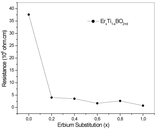
Figure 1: The electrical resistivity results of Er-doped TiBO3 samples.
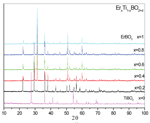
Figure 2: Comparison of XRD patterns of ErxTi1-xBO2+d samples.
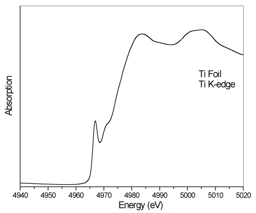
Figure 3: Ti K-edge XANES spectra of the metal Ti.
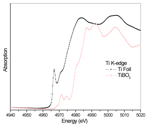
Figure 4: Compared XANES spectra of Ti K-edges of the metal Ti and TiBO3.
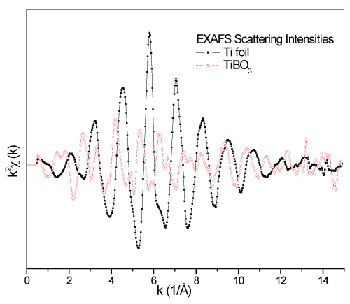
Figure 5: The comparison of the EXAFS chi data for Ti foil and TiBO3.
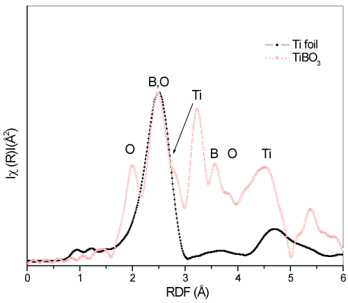
Figure 6: Compared RDF results of the Ti foil and TiBO3.
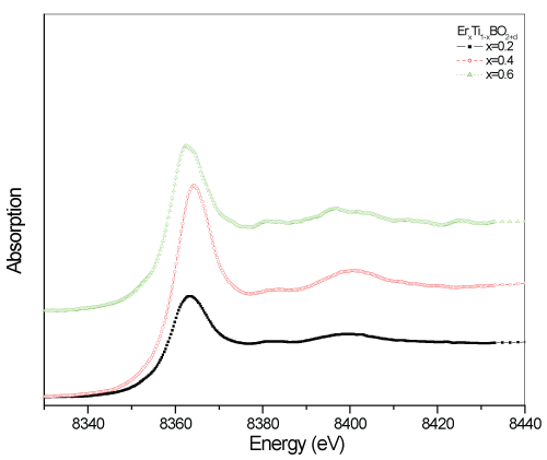
Figure 7: Compared Er L3-edge XANES spectra of the ErxTi1-xBO2+d samples.
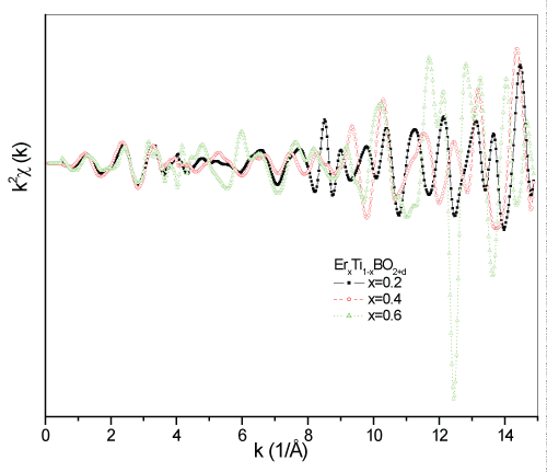
Figure 8: The comparison of the EXAFS chi scattering data for ErxTi1-xBO2+d samples.
References
-
Pitscheider A , Kaindl R, Oeckler O and Huppertz H (2011) Journal of Solid State Chemistry 184: 149-153.
-
Vink A P, Van der Kolk E, Dorenbos P and Van Eijk CWE (2004) Quantum Phospors. In: Shur MS, Zukauskas A, UV Solid-state Light Emitters and Detectors. Kluwer Academic, Dordrecht.
-
Kamiya S and Mizuno H (2007) Practical lamp Phospors. In: Yen WM, Shionoya S, Yamamoto H, Practical Applications of Phosphors, CRC Press, Taylor & Francis Group, LLC, London.
-
Träger F (2012) Springer Handbook of Lasers and Optics. Springer-Verlag, Berlin Heidelberg 623.
-
Zeng QD and Li RK (2014) Solid State Sciences 29: 75-78
-
Majchrowski A, Kityk IV and Ebothe J (2004) Phys.Status Solidi 241: 3047-3055
-
Gao R, Zhang Z and Zhao J (2014) Crystal Structures and Phase Transitions in Rare-Earth Orthoborates. Journal of the Chinese Rare Earth Society 32: 385-396
-
Liu R, Huang X, He H, Zhuang W, Hu Y and et al. (2012) Prospect and Advances of Technique and Market of Rare Earth Luminescent Materials. Journal of the Chinese Rare Earth Society 30: 265-272
-
Huppertz H (2011) New synthetic discoveries via high-pressure solid-state chemistry. Chemical Communications 47: 131-140
-
Nabi HS and Pentcheva R (2011) Energetic stability and magnetic coupling in (Cr1-xFex)2O3: Evidence for a ferrimagnetic ilmenite-type superlattice from first principles. Physical Review B 83: 214424
-
Moore Elaine A (2007) First-principles study of the mixed oxide α-FeCrO3. Physical Review B 76:195107
-
Liu YW, Rui XF, Fu YY and Han ZhangYW (2005) Synthesis of α-Fe2O3 Nanowires and its Magnetic Properties. Journal of Metastable and Nanocrystalline Materials 23:243.
-
Z Xu, MK Matam, ZG Ye (2001) American Physical Society, Annual March Meeting 2001 March 12 - 16, Washington State Convention Center Seattle, Washington Meeting ID: MAR01.
-
Ankudinov AL, Ravel B, Rehr JJ and Conradson SD (1997) Relativistic calculations of spin-dependent x-ray-absorption spectra. Phys Rev B 56: R1712
-
Ravel B, (2001) ATOMS: crystallography for the X-ray absorption spectroscopist. Journal of Synchrotron Radiation 8: 314-316.
-
Ravel B, Newville M, (2005) ATHENA, ARTEMIS, HEPHAESTUS: data analysis for X-ray absorption spectroscopy using IFEFFIT. Journal of Synchrotron Radiation 12: 537
-
Klysubun W, Sombunchoo P, Narupon Wongprachanukul, Tarawarakarn P, Chaiprapa J, et al. (2007) Commission and performance of x-ray absorption beamline at the Siam photon Laboratory. Nuclear Instruments and Methods in Physics Research 582: 87-89
-
Wantana Klysubun, Pongjakr Tarawarakarn, Panidtha Sombunchoo, Supat Linkhieo, Jitrin Chaiprapa, et al. (2006) X-ray absorption spectroscopy beamline at the Siam Photon Laboratory. AIP Conference Proceedings 879: 860-863
-
Lutterotti L and Bortolotti M (2003) Object oriented programming and fast computation techniques in MAUD, a program for powder diffraction analysis written in java. IUCr: Compcomm Newsletter 1: 43-50.
-
Grey IE, Li C, MacRae CM, Bursill LA (1996) Boron Incorporation into Rutile, Phase Equilibria and Structure Considerations. Journal of Solid State Chemistry127: 240-247