
Effect of Heat Treatment on Cds Thin Films by Chemical Bath Deposition
Ricardo Gonzalez Valenzuelao*, Hilda Esparza Ponce, David Trejo and Cesar Gonzalez Valenzuela
Centro de Investigación en Materiales Avanzados, Chihuahua, México
*Corresponding author
Ricardo Gonzalez Valenzuela, Centro de Investigación en Materiales Avanzados, Chihuahua, México, E-mail: [email protected]
Int J Electron Device Phys, IJEDP-1-001, (Volume 1, Issue 1), Research Article
Received: April 6, 2017
Accepted: June 21, 2017
Published: June 23, 2017
Citation: Valenzuela GR, Ponce HE, Trejo D, Valenzuela CG (2017) Effect of Heat Treatment on Cds Thin Films by Chemical Bath Deposition. Int J Electron Device Phys 1:001
Copyright: © Valenzuela GR, et al. This is an open-access article distributed under the terms of the Creative Commons Attribution License, which permits unrestricted use, distribution, and reproduction in any medium, provided the original author and source are credited.
Abstract
In recent years, the research on solar cells is focused on increasing its efficiency. The involved factors are numerous like irradiance, cell area, morphology, grain size, crystallographic phases, orientation (texture), band gap, thermal or surface treatment of the layers, etc. Through the development of the second generation of solar cells with thin films of chalcogenides, various investigations have been developed. Specifically in relation to enhancement the cell of CdS/CdTe in this work, CdS thin films for photovoltaic cells applications has been grown by chemical bath deposition over Glass [1] and Glass/ITO substrate [2]. After the deposition, thermal treatment has been applied by cadmium chloride solution 0.3 M. At the range of temperature from 400 C to 450 C under time periods of 10, 20 and 30 minutes in order to improve phase crystallization and grain size increasing. The thin films have been characterized by X-Ray Diffraction (XRD) before and after the thermal treatment. The optical transmittance was measured to the set of samples that were thermally treated over different conditions. It was found the recommended temperature and time in order to obtain good results. Also, it was observed a physical degradation in temperatures over 450 C and times longer than 20 min, when submitted to thermal treatment. This has also been noticed in the treatment with CdTe cells.
Introduction
The Sulphur Cadmium (CdS) thin films have been used in photovoltaic cells applications and reported by many authors [1-11]. The CdS has been used in thin films development as window layer while Tellurium Cadmium (CdTe) works as the absorbent layer.
An important and typical study of CdS thin films is its efficiency. The efficiency of this kind of cells is influenced by its capacity for electric charge transportation. Then, it has been reported transmittance spectra efficiency of 87% in about 550 nm. The photovoltaic efficiency is about 12% when CdS were thermally annealed in muffle at atmospheric ambient [3], while other authors reported 20% [12]. In order to improve this electric behavior, the thin films must be free of imperfections, increasing crystals size and reducing inter-grain cavities.
The production of these kinds of materials requires easier and low cost methods. For this reason, the Chemical Bath Deposition (CBD) technique is widely recommended. CBD is the analog in liquid phase of the well-known chemical vapor deposition technique in the vapor phase. In CBD, the deposition of thin films takes place from aqueous solutions at low temperatures (near room temperature) by a chemical reaction between dissolved precursors. The CBD technique is simple, works at low temperature and it has an inexpensive large area deposition. CBD is presently attracting considerable attention as it does not require sophisticated instrumentation like vacuum system and other expensive equipment [5] like other growing techniques [10,13,14].
Also, one advantage on CBD’s use is that the low temperature avoids oxidation and corrosion of metallic substrates. The operation parameters are easily controllable, too [15].
The CdS thin films present special characteristics reported in literature; once nucleation of CdS has begun on the substrate, it becomes easier for the film to grow. The crystals will continue to grow until the homogenous reaction dominates over the heterogeneous reaction [15].
The present work studies the impact of thermal treatment that is applied to the recent developed CdS thin films that are grown over simple glass and over glass/ITO substrates. These results are supported by microstructural characterization done by X-Ray analysis, AMF Morphological study and Optical performance evaluation [1,6-9, 16].
Another important reason of doing the present work is because it is well known that among the group II-VI semiconductors, chemical bath deposition of CdS is the most extensively investigated [15,17-22].
Other authors have been studying the effect of ultrasonication instead of CBD and they found improved characteristics over CdS films [23]; however, it is out of this study.
The increase in grain size and a homogeneous surface in the semiconductor type n, allows an interaction between the interface of the p-type semiconductor and n, leading an efficient generation of electron-hole pairs.
Experimental Procedure
The glass substrates were previously washed with mild soap and rinsed with water, followed by an ultrasonic bath in acetone. After that, they were washed in isopropyl alcohol, similar to other authors [1].
The CBD is a technique in which thin films are deposited on substrates immersed in dilute alkaline solution containing metal ions and the chalcogenide source. The method of deposition usually uses a complexing agent to control the slow release of metal ions (Cd2+) and Sulphur ions (S2-) in order to produce the controlled homogeneous precipitation of the film on the solid substrate [6].
Precursor solutions of CdCl2 0.05 M. Na3C6H5O7 0.5 M., KOH 0.5 M. and SC(NH2)2 0.5 M. and distilled water were poured in a baker [6]. The thin films were deposited over Glass and Glass/ITO substrates using CBD technique by 20 minutes at 70 C in order to obtain approximately 60 nm thickness films. A second deposition (under the same conditions) was realized in order to obtain a final thickness approximately of 120 nm thickness.
During the reaction, due to alkaline medium, pH must be under control in order to avoid the formation of Cd(OH)2 from ammonium dissociation [7].
The following reaction shows ions of Cd+2 and thiourea hydrolysis SC(NH2)2 with the formation of sulfide ions giving the final product of CdS, as shown:
1) CdCl2 + 2KOH → Cd (OH)2 + 2K+ + 2Cl-
2) Cd (OH)2 + Na3C6H5O7 + H2O → [Cd (C6H5O7)]- + 3Na+ + 2 OH-
3) Cd (C6H5O7)-→ Cd+2 + (C6H5O7)-
4) Cd (C6H5O7)- + SC (NH2)2 + OH → CdS or other compounds like CdCO3 + CdS, CdCO3
Four samples were prepared and identified as CDS6VA1, CDS6VA2, CDS6VB1, CDS6VB2, corresponding to the samples grown over Glass and CDS6IA1, CDS6IA2, CDS6IB1, CDS6IB2, corresponding to the samples grown over Glass/ITO.
Once the thin films were grown, their structural characteristics were studied by X-Ray Diffraction Analysis (XRD), using an Panalytical Xperpro equipment from 20° to 80° angles in steps of 0.05 and scanning times of 2.5 sec. [1,7,9].
The optical transmittance evaluation was done by UV-VIS Scan, using UV-Vis Perkin Elmer Lambda 10 equipment in a wavelength interval of 300 to 1000 nm.
The morphological study was performed by Atomic Force Microscopy (AFM) with a Multimode, Veeco Instrument. All the samples were evaluated under these 3 methods just after they were grown.
Once they were analyzed, a thermal treatment was performed into an air atmosphere in a range of temperature from 400 C to 450 C under time periods of 10, 20 and 30 min. This thermal procedure was compared to others reported in bibliography [6].
The XRD, optical transmittance and morphology analysis were done again.
Results and Discussion
The XRD studies revealed that all the deposited films were polycrystalline with hexagonal structure and exhibited (002) preferential orientation [6].
The XRD analysis that was done just after the samples were grown shows a very noisy signal. The planes (222) are related to the presence of ITO, while the planes (200), (220) and (311) belong to the CdS in cubic phase [3,5,9,12].
This behavior is according to expected due to the very small grain and crystal size of the sample (Figure 1). However, once the thermal treatment was performed, the XRD study is able to recognize its structural features because of the increased grain and crystal size.
The increase in crystal size after the thermal treatment reveals the presence of the main crystallographic planes ITO(211), (222) and (400) at 21.6°, 30.3° and 35.6°, respectively. While the CdS is identified by the presence of the planes (100), (002) and (101) at 24.9°, 26.6° and 28.3°, respectively, according to the proper information found in bibliography (Figure 2).
The angles and planes are supported on information reported in literature [11] (Table 1).
Later, the optical transmittance showed a regular behavior where the transmittance is proportional inversely to the incident energy, according to expected for a semiconductor. “Where the film thickness is maximum, the optical band gap is minimum” [15]. It is also reported an inverse relationship between energy gap and grain size [15]; in which, the CdS deposited over Glass shows a notorious slope change between a specific energy range. This slope change obeys to an energy absorption variation when the energy value is very close to the valence and conductive band. When this happens, the energy is able to promote an electron from valence band to conductive band, “jumping” the energy gap known as the forbidden energy band (Figure 3). This transmittance or absorbance observation allows the present study to identify the material as a semiconductor.
Besides this analysis, the sample that was deposited over the Glass/ITO substrate shows 2 different slope changes. This result is also according to expected, due to the 2 different components (ITO and CdS) present in the thin film (Figure 4).
The transmissivity spectra data is reported in literature, too [1,6,15].
As discussed before, the improved properties of the thin films is because of the crystal size increasing. This morphological change is visually observed in Figure 5, where the crystal size is bigger after several treatments as follows: The first picture shows the morphological state before any thermal treatment. The thermal treatment was done at 400 C at different time intervals. The following pictures show its new morphological situation after 10, 20 and 30 minutes, respectively. It is clear seen how the grain size is increased considerably for about 10 times, achieving particle sizes of about 100 nm width. Similar pictures are reported for other authors [3].
As mentioned before, the goal of this work is the evaluation of the effect of the thermal treatment applied to thin films of CdS deposited on ITO. The optical transmittance showed an improved behavior before 30 minutes of treatment. However, over this time, it was observed that the optical transmittance has changed considerably, evidencing a material degradation. This material degradation has been proved based on the morphological analysis, too (Figure 6).
Conclusions
This article demonstrates that CdS films were developed by CBD technique over glass and glass/ITO substrates, successfully. All samples showed good optical properties because its measured transmittance was more than 80% from 400 nm to beyond 1000 nm. The thermal treatment applied to conditions of 400 C and 10 minutes was the optimal formulation in order to get the best results. The structural and morphological study reveals that the thermal treatment offers a good alternative to photovoltaic cells of CdS because of the increased grain size. A very important finding was how long the temperature was applied; it was found that 30 min was the optimum. But also, although the material is big enough to improve its main behavior, the grain now is overly big to keep united to the substrate, causing an undesirable physical condition.
Acknowledgements
Centro de Investigacion en Materiales Avanzados. Chihuahua, Mexico.
Figures
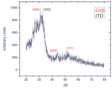
Figure 1: XRD pattern of CdS on ITO as was deposited by chemical bath deposition.
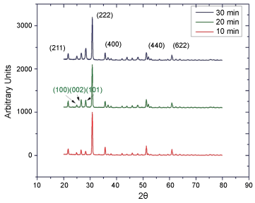
Figure 2: XRD pattern of CdS on ITO after thermal treatment to a 400 C for 10, 20 and 30 minutes.
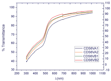
Figure 3: Plots% transmittance for thin films of CdS deposited on glass.
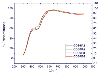
Figure 4: Plots% transmittance for thin films of CdS deposited on glass/ITO.
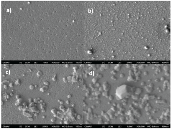
Figure 5: SEM images a) Before thermal treatment and after thermal treatment at 400 C for; b) 10 minutes; c) 20 minutes and; d) 30 minutes.
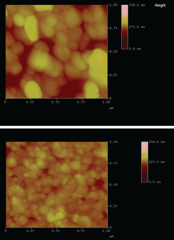
Figure 6: Morphology by AFM between CdC deposited on a) Glass and; b) Glass/ITO.
References
-
Bharat N Patil, DB Naik, VS Shrivastava (2011) Synthesis and characterization of al doped CdS thin films grown by chemical bath deposition method and its application to remove dye by photocatalytic treatment. Chalcogenide Letters 8: 117-121.
-
K Lingeswaran, SS Prasad Karamcheti, M Gopikrishnan, G Ramu (2014) Preparation and characterization of chemical bath deposited CdS thin film for solar cell. Middle-East Journal of Scientific Research 20: 812-814.
-
JM Flores Marquez, ML Albor Aguilera, Y Matsumoto Kuwabara, Ma Gonzalez Trujillo, C Hernandez Vasquez, et al. (2015) Improving Cds/CdTe thin film solar cell efficiency by optimizing the physical properties of CdD with the application of thermal and chemical treatments. Thin Solid Films 582: 124-127.
-
Hani Khallaf, Isaiah O Oladeji, Guangyu Chai, Lee Chow (2008) Characterization of CdS thin films grown by chemical bath deposition using four different cadmium sources. Thin Solid Films 516: 7306-7312.
-
Mohammad M Ali (2001) Characterization of ZnO thin films grown by chemical bath deposition. Journal of Basrah Researches 37.
-
Fouad Ouachtari, Ahmed Rmili, Sidi El Bachir Elidrissi, Ahmed Bouaoud, Hassan Erguig, et al. (2011) Influence of bath temperature, deposition time and [S]/[Cd] ratio on the structure, surface morphology, chemical composition and optical properties of CdS thin films elaborated by chemical bath deposition. Journal of Modern Physics 2: 1073-1082.
-
H Ilchuk, P Shapoval, V Kusnezh (2001) Chemical surface deposition of CdS ultra-thin films from aqueous solutions. Solar Cells Thin-films Technologies.
-
Awodugba Ayodeji Oladiran, Adedokun Oluwaseun, Sanusi Yekinni Kolawole (2012) Study of optical and crystallographic properties of CBD grown CdS thin films. IJRRAS 12.
-
S Rajpal, V Bandyopadhyay (2013) Structural and optical properties of CdS thin film grown by chemical batch deposition. Journal of Nano and Electronic Physics 5.
-
YC Goswami, Rajeev Singh, Ranjana Sharma, D Kumar (2012) Optical characterization of Cadmium Sulphide films grown by newly modified hot substrate chemical bath colloidal route. Contemporary Engineering Sciences 5: 1-8.
-
Be Xuan Hop, Ha Van Trinh, Khuc Quang Dat, Phung Quoc Bao (2008) Growth of CdS thin films by chemical bath deposition technique. VNU Journal of Science, Mathematics-Physics 24: 119-123.
-
NM Shah (2014) Structural and optical properties of Cadmium Shulphide thin films grown using chemical bath deposition. International Journal of Chem Tech Research 6.
-
AI Oliva, R Castro Rodríguez, O Solís Canto, Víctor Sosa, P Quintana, et al. (2003) Comparison of properties of CdS thin films grown by two techniques. Applied Surface Science 205: 56-64.
-
F Lisco, A Abbas, JW Bowers, G Claudio, PM Kaminski, et al. (2014) Electrodeposition of CdTe films on CdS layers deposited using magnetron sputtering and chemical bath deposition. Loughborough University, The Solar Energy Society, 23: 145-148.
-
Hani M Khallaf (2009) Chemical bath deposition of group II-VI semiconductor thin films for solar cells applications. Dissertation University of Central Florida.
-
Ch Kiran Kumar, Nguyen Thi Quynh Hoa, Soon Gil Yoon, Eui Tae Kim (2009) Highly photoconductive CdS thin films synthesized by using chemical bath deposition. Journal of the Korean Physical Society.
-
Kassim, Ho Soon Min, Tan Wee Tee, Yazid Rosli (2011) Preparation and characterization of chemical bath deposited NiSe thin films. Ozean Journal of Applied Sciences 4.
-
Busarin Noikaew, Panita Chinvetkitvanich, Intira Sripichai, Chanwit Chityuttakan (2008) The influence of growth conditions on the chemical bath deposited ZnS thin films. Journal of Metals Materials and Minerals 18: 49-52.
-
EI Ugwu, HU Igwe, DU Onah, NN Nwafor (2013) Optimization of optical properties of annealed Cadmium Selenide (CdSe) thin films grown by chemical bath deposition technique. Advances in Physics Theories and Applications 18.
-
IA Karipera, Ö Baglayanb, F GÖdec (2015) Fabrication and optical characterization of CdSe thin films grown by chemical bath deposition. Acta Physica Polonica A 128: 219-221.
-
IA Ezenwa (2013) Effect of film thickness on the transmissivity of chemical bath synthesized PbS thin film. Research Journal of Engineering Sciences 2: 23-25.
-
MD Jeroh, DN Okoli (2012) Optical, Structural and morphological studies of chemical bath deposited Antimony Sulphide thin film. Global Journal of Science Frontier Research 12.
-
Jun Young Choi, Kang Jin Kim, Ji Beom Yoo, Donghwan Kim (1998) Properties of Cadmium Sulfide thin films deposited by chemical bath deposition with ultrasonication. Solar Energy 64: 41-47.