
International Journal of Optics and Photonic Engineering
(ISSN: 2631-5092)
Volume 3, Issue 2
Research Article
DOI: 10.35840/2631-5092/4512

Article Formats
Coupling Dynamics of All-Optical Memory Cell Based on Active Micro Ring Optical Integrator with LWI and EIT Phenomena
Table of Content
Figures
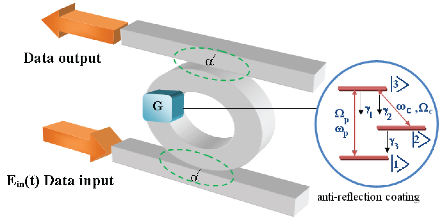
Figure 1: An optical integrator with three level....
An optical integrator with three level Λ-type QD as the gain segment.
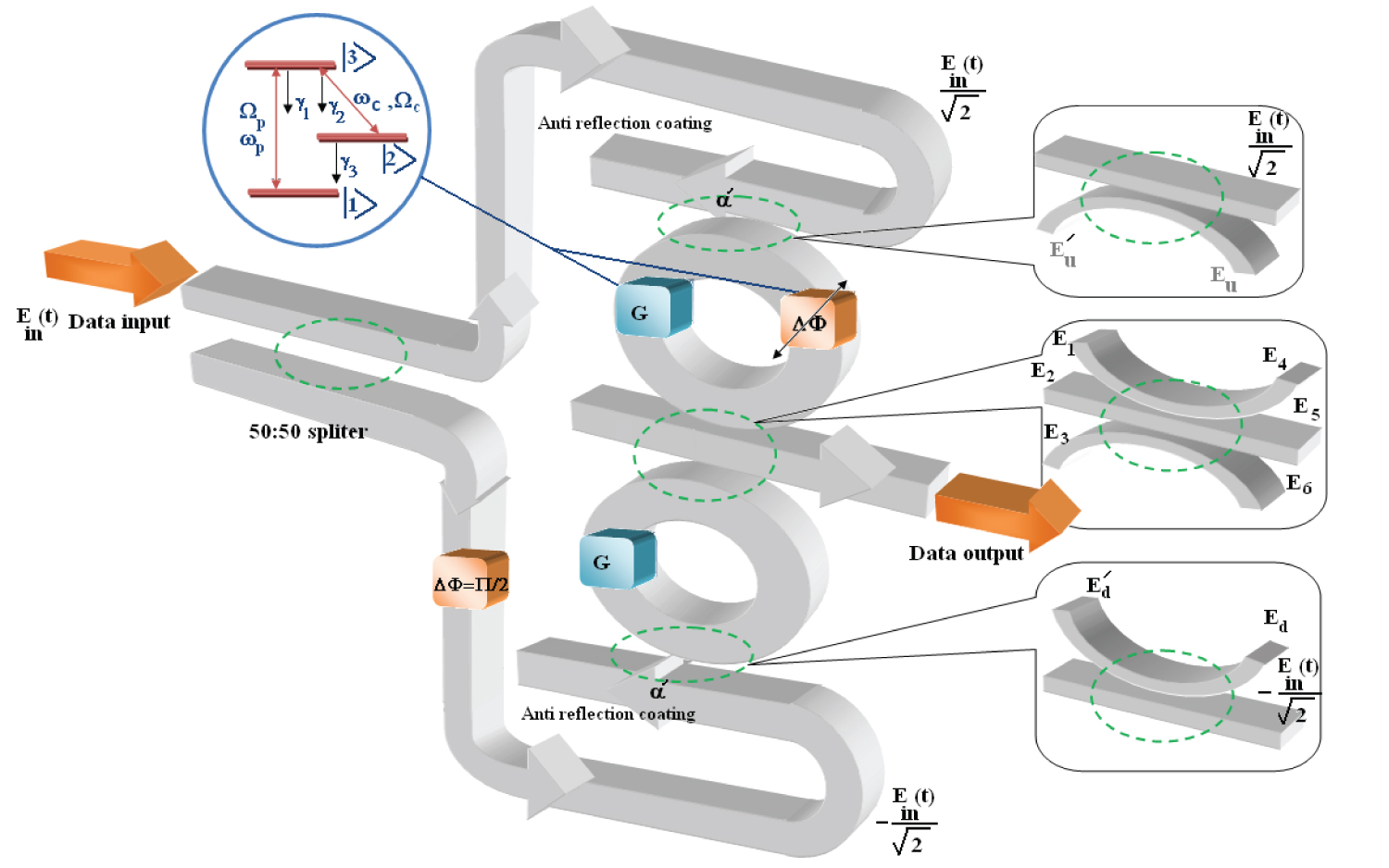
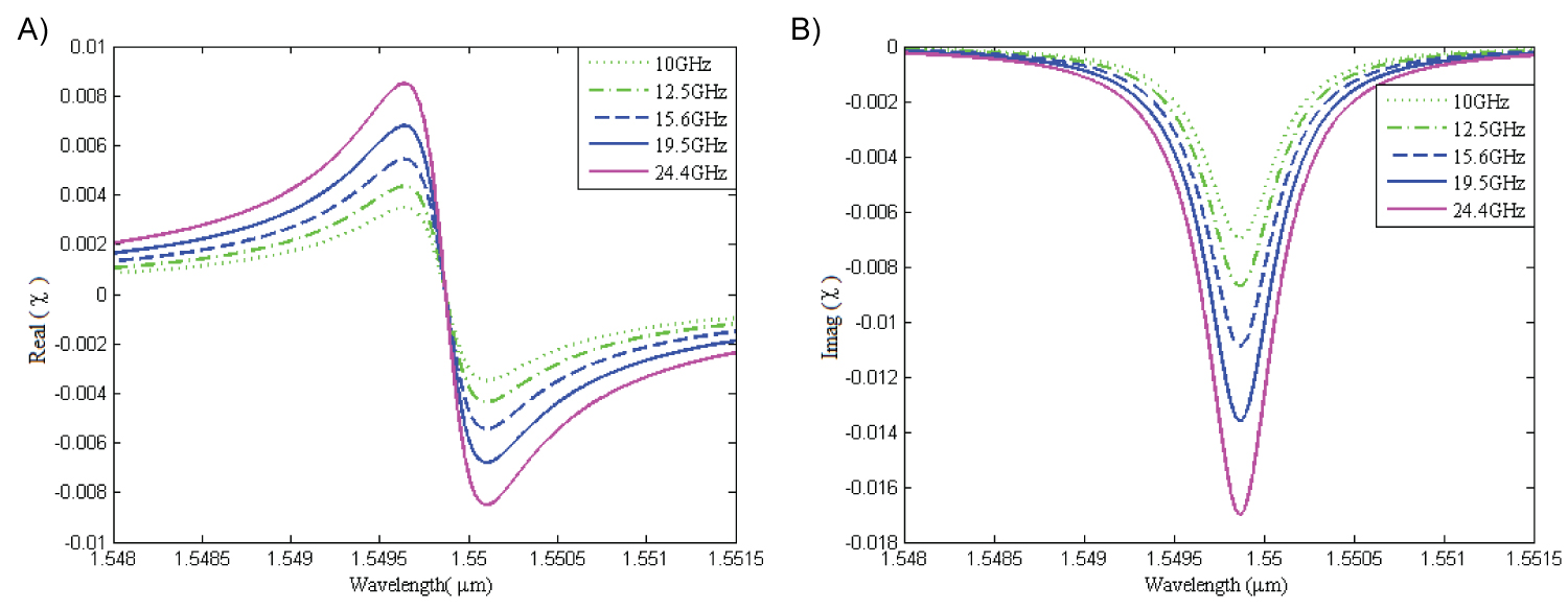
Figure 3: a) Real; b) Imaginary parts of the susceptibility for...
a) Real; b) Imaginary parts of the susceptibility for the doped 3 level QDs (Gain segments) versus wavelength for the pumping rates (10, 12.5, 15.6, 19.5 and 24.4 GHz).
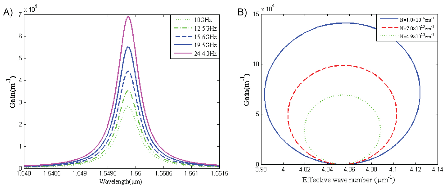
Figure 4: The LWI gain profile a) For different values of the...
The LWI gain profile a) For different values of the pumping rate; b) For different numbers of nanoparticles per unit volume.
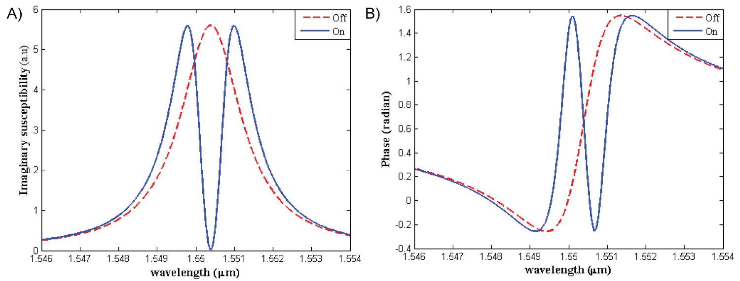
Figure 5: The phase shifter profile based on EIT a) Transparency;...
The phase shifter profile based on EIT a) Transparency; b) Phase profiles of the phase shifter segment for two cases of with and without control field.
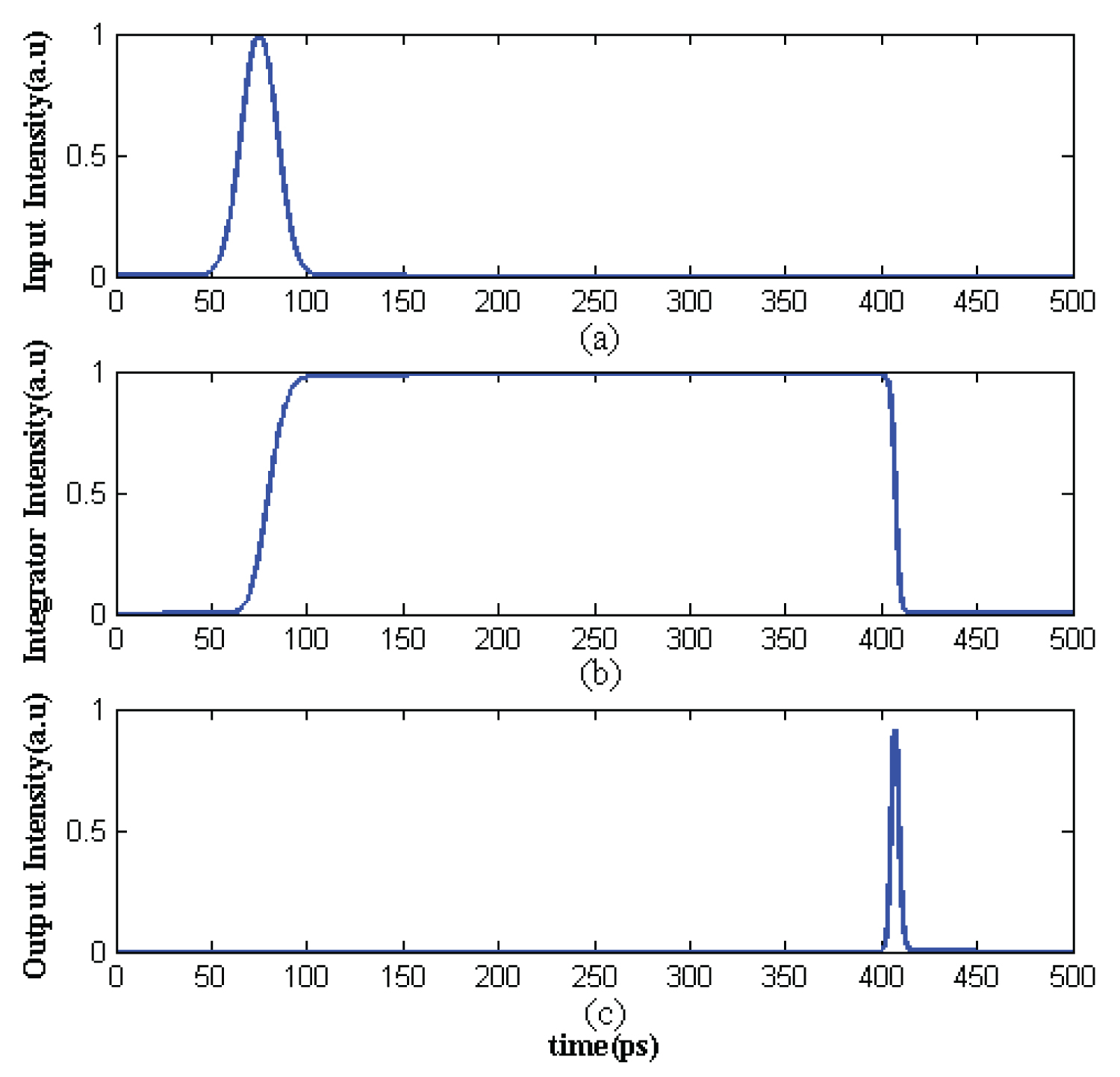
Figure 6: Data storing and read out process of optical memory unit...
Data storing and read out process of optical memory unit cell, a) Input pulse; b) Saved data; c) Output pulse. Power coupling coefficient (α = 0.5), refractive index of the fiber n = 2.8, λ = 1550 nm, length of rings L = 1 µm.
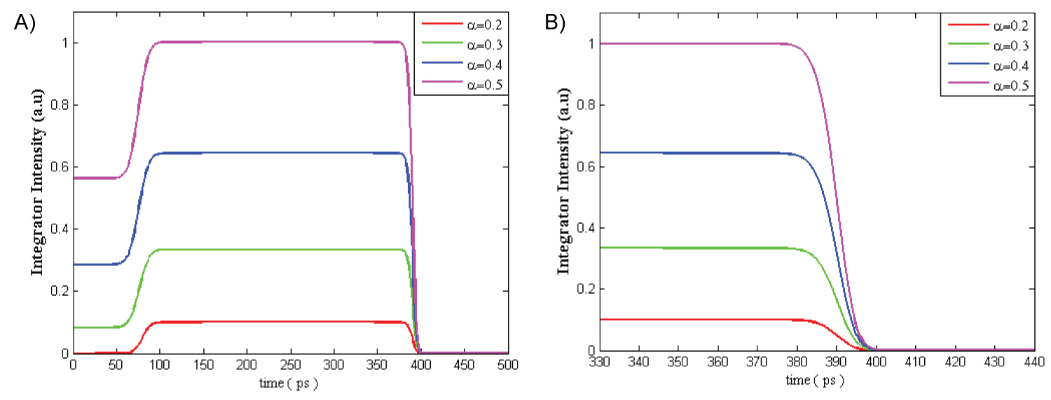
Figure 7: a) Different light fields in the optical integrator with...
a) Different light fields in the optical integrator with different power coupling coefficient of the 2 × 2 directional couplers; b) Optical integrator intensity in read out process.
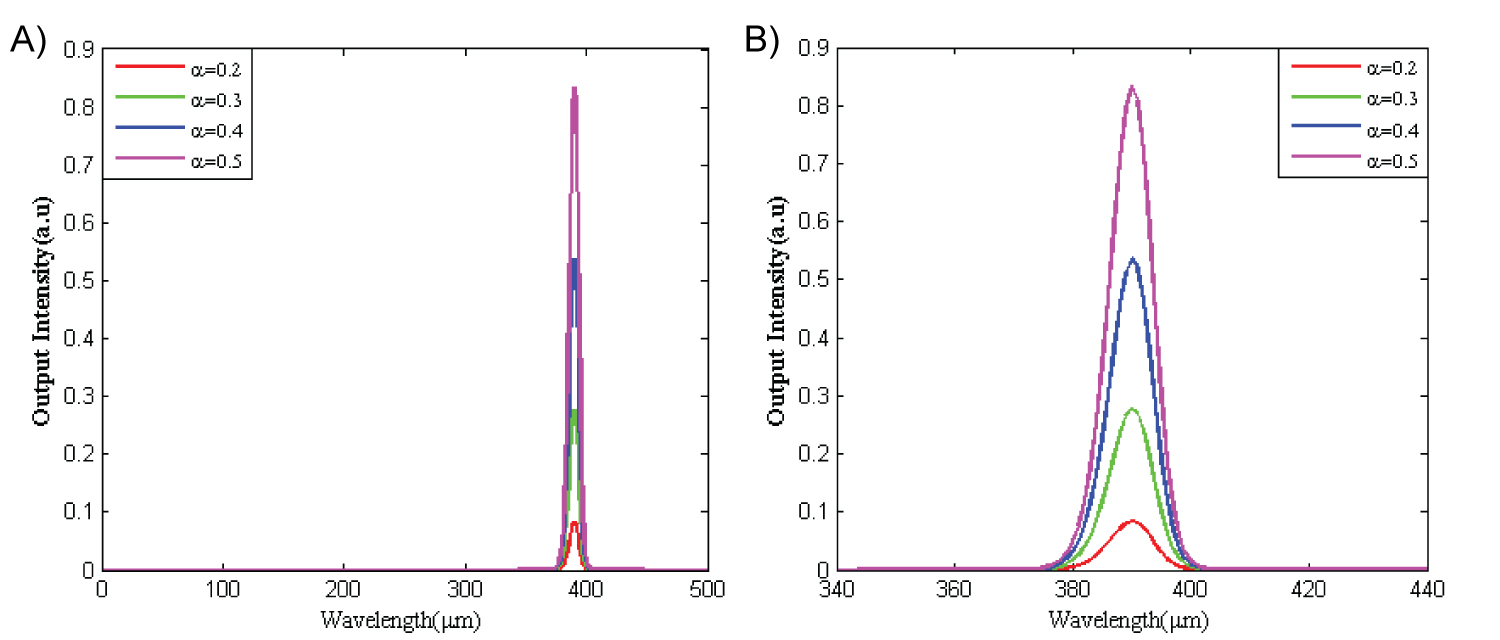
Figure 8: a) Different output pulses obtained with different...
a) Different output pulses obtained with different power coupling coefficient of the 2 × 2 directional coupler; b) The zoom out of the output pulses from the memory cell.
References
- Xu QF, Dong P, Lipson M (2007) Breaking the delay-bandwidth limit in a photonic structure. Nature Physics 3: 406-410.
- Fu SN, Shum P, Ning G, Wu CQ, Li YJ (2007) Theoretical investigation of dual-Wavelength packet signal storage with SOA-based dual loop optical buffer. Optics Communication 279: 255-261.
- Reis C, Maziotis A, Kouloumentas C, Stamatiadis C, Calabretta N, et al. (2011) All-optical clocked D flip-flop memory using a hybrid integrated S-R latch. Microwave and Optical Technology Letters 53: 1201-1204.
- Fitsios D, Vyrsokinos K, Miliou A, Pleros N (2012) Memory speed analysis of optical ram and optical flip-flop circuits based on coupled SOA-MZI gates. IEEE Journal of Selected Topics in Quantum Electronics 18: 1006-1015.
- Sahu S, Raman Pal R, Dhar S (2011) Implementation of 1-Bit random access memory cell in all-optical domain with non-linear material. International Journal of Optics and Applications 1: 8-12.
- G Mourgias-Alexandris, Ch Vagionas, A Tsakyridis, P Maniotis, N Pleros (2018) All-optical 10Gb/s ternary-CAM cell for routing look-up table applications. Opt Express 26: 7555-7562.
- Narmadhadevi P, Shanmuga Sundar D, Malathi L (2013) Performance analysis of different micro ring resonators based on optical delay lines. International Journal of Computer Applications 67: 0975-8887.
- Elshaari AW, Aboketaf A, Preble SF (2010) Controlled storage of light in silicon cavities. Optics Express 18: 3014-3022.
- Tucker RS, Riding JL (2008) Optical ring-resonator random-access memories. Journal of Lightwave Technology 26: 320-328.
- Dong B, Cai H, Gu YD, Yang ZC, Jin YF, et al. (2015) Nano-optomechanical static random access memory (SRAM). 28th IEEE International Conference on Micro Electro Mechanical Systems (MEMS) Estoril, Portugal, 49-52.
- Ding Y, Zhang X, Zhang X, Huang D (2008) Proposal for loadable and erasable optical memory unit based on dual active microring optical integrators. Optics Communications 281: 5315-5321.
- DingY, Zhang X, Zhang X, Huang D (2009) Active microring optical integrator associated with electroabsorption modulators for high speed low light power loadable and erasable optical memory unit. Opt Express 17: 12835-12848.
- Dahlem MS, Holzwarth CW, Smith HI, Ippen EP, Popović MA (2010) Dynamical slow light cell based on controlled far-field interference of microring resonators. OSA Publishing.
- Alavi SE, Amiri IS, Idrus SM, Supa'at ASM, Ali J (2013) Chaotic signal generation and trapping using an optical transmission link. Life Science Journal 10: 186-192.
- Amiri IS, Ahmad H, Al-Khafaji HM (2015) Full width at half maximum (FWHM) analysis of solitonic pulse applicable in optical network communication. American Journal of Networks and Communications 4: 1-5.
- Yanfei Tu, Guoquan Zhang, Zhaohui Zhai, Jingjun Xu (2009) Angular multiplexing storage of light pulses and addressable optical buffer memory in Pr3+:Y2SiO5 based on electromagnetically induced transparency. Physical Review A 80: 033816.
- Gouraud B, Maxein D, Nicolas A, Morin O, Laurat J (2015) Demonstration of a memory for tightly guided light in an optical nano fiber. Phys Rev Lett 114: 180503.
- Lijun Ma, Oliver Slattery, Xiao Tang (2018) Optical quantum memory based on electromagnetically induced transparency. Journal of Optics 19: 1-47.
- Ding D-S, Zhang W, Zhou Z-Y, Shi S, Shi B-S, et al. (2015) Raman quantum memory of photonic polarized entanglement. Nature Photonics 9: 332-338.
- Ding D-S, Zhang W, Zhou Z-Y, Shi S, Xiang G-Y, et al. (2015) Quantum storage of orbital angular momentum entanglement in an atomic Ensemble. Phys Rev Lett 114: 050502.
- Junling Long, HS Ku, Xian Wu, Xiu Gu, Russell E Lake, et al. (2018) Electromagnetically induced transparency in circuit quantum electrodynamics with nested polariton states. Phys Rev Lett 120: 083602.
- Scully MO, Zubairy MS (1997) Quantum optics. Cambridge University Press, Cambridge, New York.
- Kowalski K, Long V, DinhXuan K, Glodz M, Nguyen B, et al. (2010) Electromagnetically induced transparency. Computational Methods in Science and Technology, 131-145.
- N Pasyar, R Yadipour, H Baghban (2017) Design of all-optical memory cell using EIT and lasing without inversion phenomena in optical micro ring resonators. Optics communications 395: 241-248.
- Zhang XB, Huang DX, Zhang XL (2007) Transmission characteristics of dual microring resonators coupled via 3×3 couplers. Optics Express 15: 13557-13573.
Author Details
Nasibe Pasyar*
Faculty of Electrical and Computer Engineering, University of Tabriz, Tabriz, Iran
Corresponding author
Nasibe Pasyar, Faculty of Electrical and Computer Engineering, University of Tabriz, Tabriz, Iran, Tel: 5166615813.
Accepted: November 08, 2018 | Published Online: November 10, 2018
Citation: Pasyar N (2018) Coupling Dynamics of All-Optical Memory Cell Based on Active Micro Ring Optical Integrator with LWI and EIT Phenomena. Int J Opt Photonic Eng 3:012.
Copyright: © 2018 Pasyar N. This is an open-access article distributed under the terms of the Creative Commons Attribution License, which permits unrestricted use, distribution, and reproduction in any medium, provided the original author and source are credited.
Abstract
The lasing without inversion phenomena in the three-level nanoparticles inserted in the micro ring resonators as the active gain medium for loss compensation in the all-optical memory unit cell is investigated. The effect of parameters such as pumping rate is analyzed. Also, the electromagnetically induced transparency effect in the three-level quantum dots is utilized as an on/off phase shifter for data reading at requested time. The optical integrator generates an optical step function to save the input data. Both the input data into the memory and the output read out are the return-to-zero Gaussian signals. Since, the light in the integrator is mostly erased during the rising edge of the phase shift pulse, the output data has the narrower pulse width. Finally, the effect of the power coupling coefficient of the directional couplers on data storage and read out process is investigated. Device minimizing for integrated purposes and high-speed data saving are the main advantages of the optical integrator-based memory.
Keywords
Ring resonator, All-optical memory cell, 3 × 3 coupler, Electromagnetically induced transparency, Lasing without inversion, Coupling coefficient
Introduction
The optical memory, as an important element in the future all optical computing and all optical networks, is attracting wide attention. Most of the current optical memories depend on the high nonlinear properties of the materials such as silicon, in which the optical properties can be changed upon triggered by the light [1]. However, such kind of the memory normally requires the high operating power or the complex structure. Due to the ever-increasing speed of the fiber-optic-based telecommunications, the high-speed optical memories adapted to the densely on-chip integration, become critical for buffering of the telecommunication data [2]. The all-optical memory or buffer as a key element in the optical packet switching (OPS) networks can resolve the packet contention problem. Tunable optical delay lines and optical memories as important building blocks in advanced photonic integrated circuits (PICs) will offer the possibility to combine the numerous optical functions including the switching, modulation and amplification on a single substrate for the optical information processing in the all optical communication networks. Most of the optical buffering schemes such as slowing light, the optical fiber loop and so on, produce a delay time of the data stream. The storage time in the fiber loop optical memories, can be up to 1ms. However, the setup is bulky because typically at least several meters long of fiber are required for the fiber loop [1,2].
Flip-flop memory is one kind of the most interesting memory types. However, it is still a great challenge to realize ultra-fast flip-flop operation with the switching time on the picosecond time scale for GHz data memory [3]. Two SOA-based ON/OFF switches and two coupled semiconductor optical amplifier- Mach Zender interferometer (SOA-MZI) gates forming an optical flip-flop have demonstrated an optical random access memory (RAM) cell [4]. An all-optical switch by a composite slab of linear medium (LM) and non-linear medium (NLM) has been massively used as the building block to propose 1-bit Random Access Memory (RAM) circuit. An all-optical clocked D flip flop is the main storing element of the proposed RAM with the storing and reading time of fs [5].
All-optical Ternary-Content Addressable Memory (T-CAM) cell is demonstrated that operates at 10 Gb/s and comprises two monolithically integrated InP Flip-Flops (FF) and a SOA-MZI optical XOR gate. The two FFs are responsible for storing the data bit and the ternary state 'X', respectively, with the XOR gate used for comparing the stored FF-data and the search bit. The experimental results reveal error-free operation at 10 Gb/s for both Write and Ternary Content Addressing of the T-CAM cell, indicating that the proposed optical T-CAM cell could in principle lead to all-optical T-CAM-based Address Look-up memory architectures for high-end routing applications [6].
Slow light devices have been extensively build using the coupled resonator optical waveguides (CROW) [7,8]. Random access all-optical memory unit cells are also designed using the ring resonators in which a data bit is stored in a resonator. It is shown that the losses in the resonators, the extinction ratio and the chirp of the variable coupling medium that injects and extracts data into and out of the resonators, and the chirp on the input signal are the limiting factors in the resonator-based optical memories [9]. The optomechanical effect between the silicon beam and the ring resonator is used to design the nano-optomechanical static RAM (SRAM) integrated with the light modulation system on a single silicon chip in which the bistability of the silicon beam due to the non-linear optical gradient force generated from a ring resonator determens the memory states. The optical SRAM has write/read time around 120 ns, which is much faster as compared with the traditional MEMS memory [10].
Also, a memory unit cell has been presented in [11,12] based on the micro ring resonators in which the electro absorption modulator (EAM) in the Mach Zender interferometer (MZI) form operates as an optical switch. The proposed unit cell cannot operate as an all-optical element and has large size to appear in the integrated chip [11,12]. A dynamical slow light cell with dual-microring resonator configuration and the far-field coupling has been demonstrated by controlling the group delay through thermo-optically detuning the resonant frequencies of the two rings in which the usable group delays up to 24 ps are measured, with losses < 1 dB [13].
The Micro ring resonator (MRR) has been used for chaotic signals generation and trapping along the fiber optic communication [14]. By proper selection of the parameters such as the refractive indices of a silicon waveguide, coupling coefficients, coupling loss and the input power, the nonlinear behavior can be operated. The signal trapping could be obtained after the signals were transmitted along the fiber optic and finally received by suitable optical receiver. In this case the FWHM and FSR of the trapped signals have been reported as 600 fm and 45 pm [14,15].
Electromagnetically induced transparency (EIT) has been used for slowing down light pulses to store in EIT media. By this means, multiple light pulses have been stored in Pr:YSO crystal by angular multiplexing and achieved addressable all-optical delay lines and buffer memories without cross-talk among different channels [16]. Recently, an EIT optical memory scheme based on the interaction of cold cesium atoms with the evanescent field surrounding an optical nano fiber has been proposed and experimentally demonstrated [17]. Using EIT, long storage times of greater than 1 s for quantum memory and greater than 1 min for optical memory have been demonstrated. Currently, most EIT quantum memory schemes are based on rubidium (Rb) atoms or cesium (Cs) atoms, and the corresponding operating wavelengths are 780 nm and 795 nm for Rb or 852 nm and 895 nm for Cs [18]. In comparison to EIT memory based on a warm atomic vapor, the cold atoms system can provide a much longer spin coherence time, resulting in a longer available storage time. Because it is implemented off resonance, Raman quantum memory requires a very strong control beam. The strong control beam likely causes spontaneous four-wave-mixing (SFWM), and results in a high number of noise photons that are in the same spatial, temporal and frequency mode as the retrieved signal photons [18]. The problem is particularly severe in warm atomic ensembles. Raman memory in cold atoms can eliminate large Doppler broadening and uses small off-resonant detuning and a weaker control field. Recently, Raman memory in cold atoms has been demonstrated with very low noise and has been used for non-classical light storage [19,20]. Quantum memories for photons, where non-classical states of photons are mapped onto stationary matter states and preserved for subsequent retrieval, are technical realizations enabled by exquisite control over interactions between light and matter. The ability of quantum memories to synchronize probabilistic events makes them a key component in quantum repeaters and quantum computation based on linear optics. Quantum networks will enable extraordinary capabilities for communicating and processing quantum information. These networks require a reliable means of storage, retrieval, and manipulation of quantum states at the network nodes. A node receives one or more coherent inputs and sends a conditional output to the next cascaded node in the network through a quantum channel. This basic functionality is demonstrated by using the quantum interference mechanism of electromagnetically induced transparency in a qubit coupled to a superconducting resonator. The first observation of EIT is reported using all dipole allowed transitions in a Λ-type system implemented with superconducting quantum circuit. A microwave bias is applied to the qubit-cavity system to prepare a Λ-type three-level system of polariton states. Then two interchangeable signals, a probe tone and a control tone are inserted, and it is observed that transmission of the probe tone is conditional upon the presence of the control tone that switches the state of the device with up to 99.73% transmission extinction [21].
In this paper, Electromagnetically Induced Transparency (EIT) and Lasing Without Inversion (LWI) techniques in the three level quantum dots (QDs) doped into the active microring resonators as the optical integrators in the all-optical memory unit cell are applyed to make a delay line to achieve the required phase shift and amplify the optical pulse, respectively. A single optical integrator generates an optical step function for the Gaussian input pulse [10]. The proposed dual optical integrators can realize a scheme of controllable optical memory unit with a phase shift element introduced for the data reading control, the data bit can be read out at any time needed. The compact size for densely integration and large-scale data storage and being very convenient to be cascaded are the main advantages of such optical memory unit. Secondly, the read-out response time of the read operation is very fast. The high speed operations in picoseconds scale is demonstrated. The main advantage of the optical integrator-based memory compared to the flip-flop memory, is that the rising edge is the cumulative time integral of the input pulse, so it is as fast as the bit rate, and this performance is very important for the high-speed data storage. Also, the read out time depends on whenever the phase shifter pulse is applied. Here, The effect of parameters such as pumping rate on optical susceptibility and LWI gain in three-level nanoparticles doped to the ring resonator as the active gain mediume for optical power loss in data storage is investigated and EIT technique for the required phase shift for the data read has been processed. Finally, the power coupling coefficient of 2 × 2 directional couplers in ring resonators are changed and its effect on the data storage and the pulse read out process is investigated.
Memory Design
The memory structure contains optical integrator based on a 2 × 2 direct coupler as shown in Figure 1, where, is the power coupling coefficient of the directional coupler. The field propagated in the counter clockwise direction in the resonator, is enhanced due to the positive feedback in each round-trip or the sampling period T, until all the input light pulse is injected.
Then, because of the loss compensation supplied by the active gain medium, the light intensity is still kept on. By doping the 3-level nanocrystals (quantum dots) into the gain and phase shifter segments in the ring resonator and using the LWI and EIT techniques we get the required gain and phase shift to read out the stored data. The 3-level Λ type nanoparticles doped into the ring resonator as the gain segment is illustrated in Figure 1. The control field is applied in resonant with the transition and the probe field is applied to the transition, respectively.
Electromagnetically induced transparency and LWI process
In the 3-level QD structure considered in Figure 1, the levels and are coupled by the probe field of amplitude and frequency , whose dispersion and absorption we are interested. Level is coupled to level by a strong control field of frequency . The Hamiltonian of three-level Λ-type atomic system can be written as [22]:
Where, are the probe field frequency, the control field frequency, the reduced plank constant, the energy of atomic level , the energy of atomic level , the complex Rabi frequency of the probe field coupled to atomic transition , the complex Rabi frequency of the control field coupled to atomic transition and the Hermitian conjugate, respectively.
With the substitution of where, is dipole moment element and based on the Hamiltonian, the equations of motion for the density matrix elements can be expressed as [22,23]:
Solving the coupled set of equations, the time dependent density matrix element can be written as [24]:
The linear susceptibility of the system is:
Using the relation of polarization in equation (5), and by using the density matrix approach and the rate equations, one can find the electromagnetically susceptibility of the medium as a function of the weak probe field. The imaginary part of susceptibility, determines the absorptive properties of the medium and the real part, is related to the refractive index. So, for the case of EIT by using the equations (2), (3), and (5) the following expression for real and imaginary parts of the complex optical susceptibility is obtained [22,24].
Where, are the probe field frequency, the resonance detuning of , the Rabi frequency, the vacuum dielectric constant, the reduced plank constant, the dipole moment element of , the propagation wave vector, the refractive index of the wavegiude, the optical wave velocity in vacuum, the atomic density of doped nanocrystals and the atomic decay rates, respectively.
For the analysis of lasing without inversion (LWI), a single mode field of frequency υ and complex amplitude E(t) interacts with the three-level atomic system, so the interaction Hamiltonian with some substitutions is written as the following:
In this case the equations of motion for the elements of the population matrix are given by [24]:
Where, is the pumping rate. The equation of motion for the field amplitude is given by [22,24]:
We assume E(t) to be slowly varying function of time.
For certain choices of parameters, the absorption terms proportional to and will cancel the coherence terms proportional to and leading to lasing without inversion. This happens in the case that:
and
Based on basic relations of optical susceptibility equations (6), (7) with gain and refractive index, the following relations are written [22].
Memory structure
In the all-optical memory structure illustrated in Figure 2, the gain and phase shifter segments are doped by 3-level nanoparticles to utilise EIT and LWI effects.
Two identical micro rings with the gain mediums as the optical integrators are coupled via a 3 × 3 coupler. The phase shifter in the upper integrator plays a critical role for the data writing and reading operations. The input data pulse is splitted into two beams by a lossless and polarization independent 50:50 splitter. An additional π/2 phase shift is introduced into the π/2 changed phase of the lower beam after the splitter to achive the phase difference of π between two beams. The light fields injected into the upper and lower integrators are and , respectively. The light fields stored in the upper and lower integrators are represented by E4(t) and E6(t), respectively. The output field from the memory unit is denoted by E5(t). The amplitude and the phase propagation equations can be described as [11]:
Where, and are the effective wave number of the field, the gain coefficient, the optical loss of the microring resonator and the effective refractive index, respectively.
Assuming that the location of the phase shifter is zp, the output light phase of the phase shifter and the light field in the 2 × 2 coupler satisfy the following relations [11]
Where, Eiin is the optical data stream injected into the optical integrator, and Ein is the input field at the input port of the memory unit.
The following transfer functions are considered for 3 × 3 couplers [25]:
Where, characterizes the coupling strength between the two adjacent waveguides in the 3 × 3 couplers. The 3 × 3 coupler is designed as , thus the transfer function of 3 × 3 coupler is reduced as [11,24]:
Where, and are the optical gain, the power coupling coefficient, the waveguide loss, the length of ring resonator, the angular frequency of the optical pulse, the loop delay in the ring resonator and the magnitude of phase shift in the phase shifter segment, respectively. Initially the phase shifter is adjusted to . Thus, there is no light at the output port 5 and the data is stored in the micro ring integrator and . If the phase shifter is turned to under the gain matching condition, after a round trip from port 4 (6) to 1 (3), the fields are changed and given by [11,24]:
The remaining light intensity in the integrator and output port after N round trips can be written as:
Simulation Results
This section consists of the simulation results based on the numerical investigation for the proposed all-optical memory cell. After the illustration of the optical susceptibility of three level QDs, the simulation results of the gain medium implemented by LWI effect and the phase shift realized by EIT are considered. Finally, the operation of the optical memory is illustrated and the effects of the coupling coefficient on the intensity of the stored data into the resonators and the read out pulse are investigated.
The real and imaginary parts of the optical susceptibility of the doped 3-level QDs in the case of LWI, versus wavelength are illustrated in Figure 3 for different values of the pumping rates (10, 12.5, 15.6, 19.5 and 24.4 GHz) and the parameter values of 1/cm3, .
The real part of susceptibility, in Figure 3a, is related to the refractive index and the imaginary part of susceptibility, in Figure 3b, determines the absorptive properties of medium and it is proportional to absorption and the negetive , means the existance of the gain. According to Figure 3 by increasing the pumping rates the susceptibility peaks increase.
The LWI gain profile of the gain segments in the integrators for different values of the pumping rates (10, 12.5, 15.6, 19.5 and 24.4 GHz) is illustrated in Figure 4. It is observed that by increasing the pumping rate the LWI gain increases linearly. It is clear that these gain segments in spite of amplifying the optical pulse as much as required, can operate as a sharp filter. Also, it is observed that the gain is increased by numbers of nanoparticles per unit volume.
Figure 5 illustrates the electromagnetically induced transparency (EIT) applied as an optical phase shifter with the following parameter values of the phase shifter. 1/cm3, coulomb. meter, . According to the transparency profile of the phase shifter segment in Figure 5a, in absence of the control field, the signal field, which interacts with the resonant two-level system, undergoes partial or complete absorption. By applying the control field near the resonance wavelength of 1550 nm the absorption of the signal is greatly reduced and EIT is obtained. It is obvious in Figure 5b that the required phase shift, π/2, (which is necessary for reading the stored data) can be realized in EIT window about 1550 nm wavelength by applying the control field.
The data storing and read out process of the proposed all-optical memory unit cell is illustrated in Figure 6. The input Gaussian pulse to the all-optical memory cell is presented in Figure 6a. The input pulse is saved with a step function shape in the integrators as the storage process in Figure 6b. Finally, it is observed in Figure 6c that whenever the required phase shift is occurred by applying the control field of the phase shifter segment, the stored data is read out.
By considering the Figures 6b and Figure 6c, one can see that by applying the required phase shift, the input pulse is occurred in the output port and the integrators are deleted from the data.
Since, the light in the integrator is mostly erased during the rising edge of the phase shift pulse so, the FWHM of the read-out data is about 10.5 ps, a little narrower than half of the FWHM of the phase shift pulse with a value of 21.5 ps.
Then, the power coupling coefficient of the directional couplers in the ring resonators are changed and its effect on data storage process is investigated. Figure 7 represents different optical intensities saved in the integrator with different power coupling coefficient (α = 0.2, 0.3, 0.4 and 0.5). As shown in Figure 7a, the optical intensity kept on in the optical integrator increases as the power coupling coefficient increases. However, to satisfy the gain matching condition, more gain is requaired for larger power coupling coefficient. As illustrated in Figure 7b in read out process, the saved data is eareased in a sharp slope from the integrator for larger values of α.
By applying the phase shifter pulse with the peak value of π/2, the signal saved in integrators is read out from the memory. The corresponding read out pulses with different power coupling coefficient (α = 0.2, 0.3, 0.4 and 0.5) are shown in Figure 8. The larger amplitude of read out pulses is emerged by increasing the coupling coefficient. From Figure 8, we can find that the power coupling coefficient only impacts the amplitude rather than the shape of the read out pulse. According to Figure 8b, the output pulse width is remained unchanged for different values of α.
Conclusions
The LWI phenomena in 3-level QDs inserted in both resonators in the memory unit cell to realize active gain medium is investigated. The real part of susceptibility relating to the refractive index and the imaginary part of susceptibility representing the absorptive properties of the medium are changed by increasing the pumping rate. So, the LWI gain is increased as the pumping rate increases. Also, the EIT phenomena is realized to achieve the required phase shift for pulse read out process. The data write and read out process of the proposed all-optical memory unit cell are illustrated. Finally, it is observed that the optical intensity kept on in the optical integrator increases as the power coupling coefficient of the directional couplers increases, corresponding to the output pulse with larger amplitude. The high speed operation and the device minimizing for the integrated purposes are the main advantages of the proposed memory cell.