International Journal of Optics and Photonic Engineering
(ISSN: 2631-5092)
Volume 4, Issue 1
Research Article
DOI: 10.35840/2631-5092/4515

Article Formats
Proposal of 1 × 8 and 8 × 1 All-Optical Controllable Switch Arrays by Dipole Induced Transparency Applicable in DWDM
Table of Content
Figures
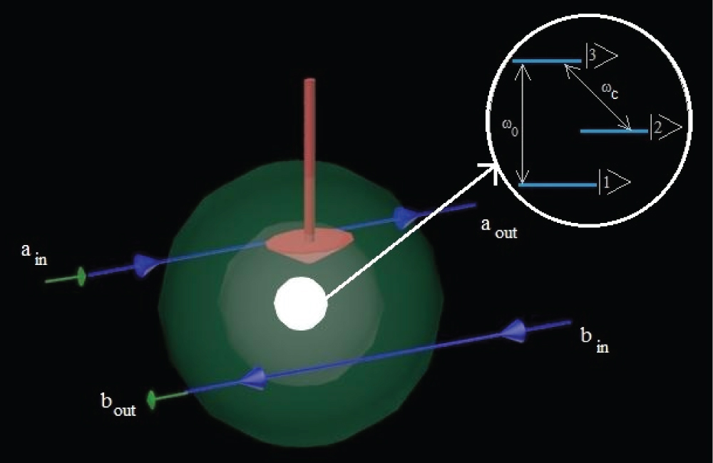
Figure 1: PC-QED cavity-waveguide switch...
PC-QED cavity-waveguide switch system, including schematic of a Λ type 3-level nano crystal doped in PC cavity.
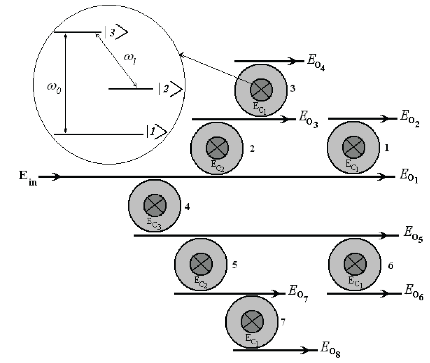
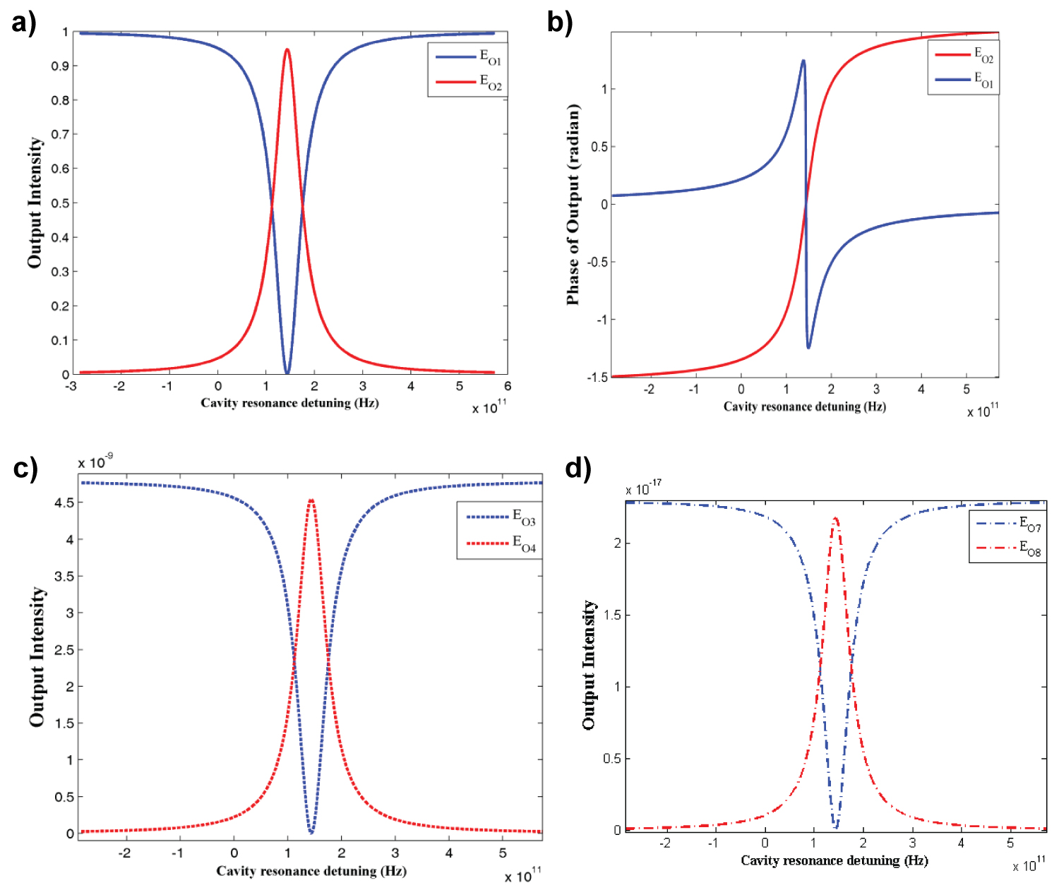
Figure 3: Optical pulse propagation in 1 × 8 switch...
Optical pulse propagation in 1 × 8 switch with only Ec1 on. a) The outputs of the first PC-QED cavity; b) The phase of these outputs; c) The outputs of the third and fifth cavity; d) The output of the seventh cavity.
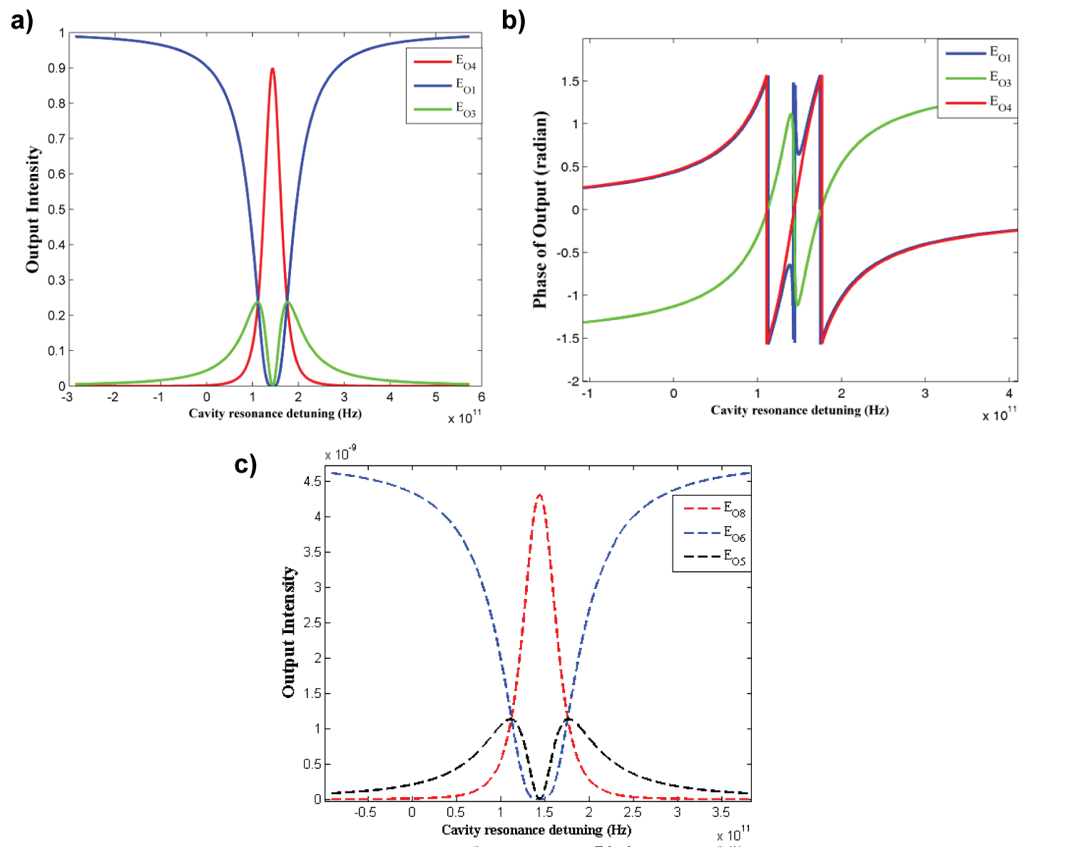
Figure 4: Optical pulse propagation for the...
Optical pulse propagation for the case of both Ec1 and Ec2 are on. a) The outputs of the first, second and third PC-QED cavity; b) The phase of outputs; c) The outputs of fourth, fifth, sixth and seventh PC-QED cavity.
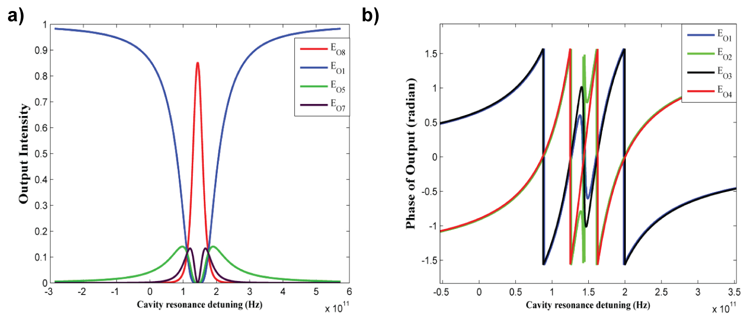
Figure 5: Optical pulse propagation for the...
Optical pulse propagation for the case of all Ec1, Ec2, and Ec3 are on. a) The outputs for all of the PC-QED cavities; b) The phase of these outputs.
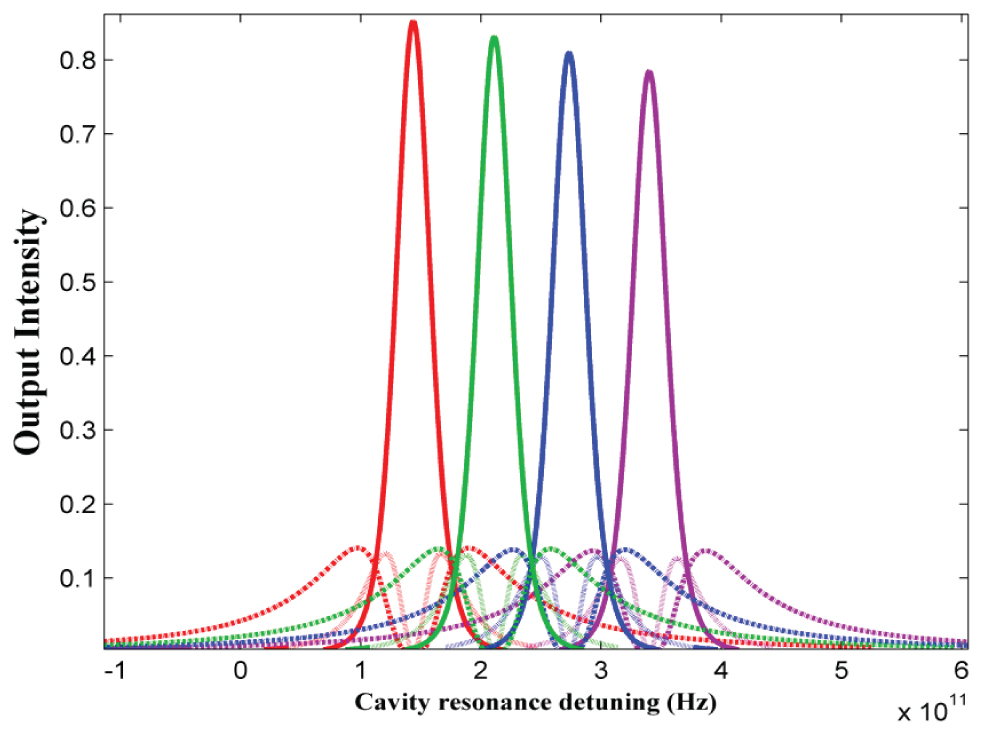
Figure 6: Pulse propagation for different...
Pulse propagation for different wavelengths. Red lines for Ec = 2.63 × 10⁴ v/m, green lines for Ec = 2.17 × 10⁴ v/m, blue lines for Ec = 1.9 × 10⁴ v/m and purple lines for Ec = 1.71 × 10⁴ v/m.
References
- Sang-Mook Lee, Ki-Man Choi, Sil-Gu Mun, Jung-Hyung Moon, Chang-Hee Lee (2005) Dense WDM- PON based on wavelength-locked Fabry -Pe/spl acute/rot laser. IEEE Photonics Technology Letters 17: 1579-1581.
- Yang Di, Wang Yi-quan, LV Mi, Chen Shao-wu, YU Jin-zhong (2007) A 2 × 2 SOI mach- zehnder thermo optical switch based on strongly guided paired multimode interference couplers. Optoelectronics Letters 3: 334-336.
- Yong-Kee Yeo, Zhaowen Xu, Dawei Wang, Jianguo Liu, Yixin Wang, et al. (2009) High- speed optical switch fabrics with large port count. Opt Express 17: 10990-10997.
- H Gibbs (1985) Optical bistability: Controlling light with light academic. New York.
- RP Schreieck, MH Kwakernaak, H Jaeckel, H Melchior (2002) All-optical switching at multi-100-Gb/s data rates with Mach-Zehnder Interferometer Switches. IEEE J Quantum Elec 38: 1053-1061.
- H Nakamura, S Nishikawa, S Kohmoto, K Kanamoto, K Asakawa (2003) Optical nonlinear properties of InAs quantum dots by means of transient absorption measurements. J Appl Phys 94.
- T Guenther, C Lienau, T Elsaesser, M Glanemann, VM Axt, et al. (2002) Coherent Nonlinear Optical Response of Single Quantum Dots Studied by Ultrafast Near-Field Spectroscopy. Phys Rev Lett 89: 057401.
- R Prasanth, JEM Haverkort, JH Wolter (2003) Electrorefraction in quantum dots: Dependence on lateral size and shape. Proceeding IEEE-Nano, San Francisco, USA, 1: 126-129.
- MA Anto'n, Oscar G Caldero'n, Sonia Melle, I Gonzalo, F Carren˜o (2006) All- optical switching and storage in a four-level tripod-type atomic system. Optics Communications 268: 146-154.
- S Rebic, D Vitali, C Ottaviani, P Tombesi, M Artoni, et al. (2004) Polarization phase gate with a tripod atomic system. Phys Rev A 70: 032317.
- E Waks, J Vuckovic (2006) Dipole induced transparency in drop-filter cavity-waveguide systems. Phys Rev Lett 96: 153601.
- Ta'eed VG, Lamont MR, Moss DJ, Eggleton BJ, Choi DY, et al. (2006) All optical wavelength conversion via cross phase modulation in chalcogenide glass rib waveguides. Opt Express 14: 11242-11247.
- Peter Bermel, Alejandro Rodriguez, Steven G Johnson, John D Joannopoulos, Marin Soljačić (2006) Single photon all-optical switching using waveguide-cavity quantum electrodynamics. Phys Rev A 74: 043818.
- MA Antón, F Carreño, Oscar G Calderón, S Melle, I Gonzalo (2008) Optical switching by controlling the double-dark resonances in a N-tripod five-level atom. Optics Communications 281: 6040-6048.
- Wen-Xi Lai, Hong-Cai Li, Rong-Can Yang (2008) Controlled optical switching based on dipole-induced transparency in a cavity-waveguide system. Optics Communications 281: 4048-4053.
- Edo Waks, Jelena Vuckovic (2006) Dispersive properties and large Kerr nonlinearities using dipole- induced transparency in a single-sided cavity. Phys Rev A 73: 041803.
- MO Scully, MS Zubairy (1997) Quantum optics. Cambridge University Press, USA.
- Jingjing Zhang, Sanshui Xiao, Claus Jeppesen, Anders Kristensen, Niels Asger Mortensen (2010) Electromagnetically induced transparency in metamaterials at near-infrared frequency. Opt Express 18: 17187-17192.
- Baur S, Tiarks D, Rempe G, Dürr S (2014) Single photon switch based on rydberg blockade. Phys Rev Lett 112: 073901.
- Shomroni I, Rosenblum S, Lovsky Y, Bechler O, Guendelman G, et al. (2014) All-optical routing of single photons by a one-atom switch controlled by a single photon. Science 345: 903-906.
- Chen W, Beck KM, Bücker R, Gullans M, Lukin MD, et al. (2013) All-optical switch and transistor gated by one stored photon. Science 341: 768-770.
- Souza JA, Figueroa E, Chibani H, Villas-Boas CJ, Rempe G (2013) Coherent control of quantum fluctuations using cavity electromagnetically induced transparency. Phys Rev Lett 111: 113602.
- Chaneliere T, Matsukevich DN, Jenkins SD, Lan SY, Kennedy TAB, et al. (2005) Storage and retrieval of single photons transmitted between remote quantum memories. Nature 438: 833-836.
- Tiarks D, Schmidt S, Rempe G, Dürr S (2016) Optical π phase shift created with a single-photon pulse. Sci Adv 2: e1600036.
- Beck KM, Hosseini M, Duan Y, Vuletić V (2016) Large conditional single-photon cross-phase modulation. Proc Natl Acad Sci USA 113: 9740-9744.
Author Details
Nasibe Pasyar*
Faculty of Electrical and Computer Engineering, University of Tabriz, Tabriz, Iran
Corresponding author
Nasibe Pasyar, Faculty of Electrical and Computer Engineering, University of Tabriz, Tabriz, 5166615813, Iran.
Accepted: January 23, 2019 | Published Online: January 25, 2019
Citation: Pasyar N (2019) Proposal of 1 × 8 and 8 × 1 All-Optical Controllable Switch Arrays by Dipole Induced Transparency Applicable in DWDM. Int J Opt Photonic Eng 4:015.
Copyright: © 2019 Pasyar N. This is an open-access article distributed under the terms of the Creative Commons Attribution License, which permits unrestricted use, distribution, and reproduction in any medium, provided the original author and source are credited.
Abstract
The proposed 1 × 8 and 8 × 1 all-optical controllable switch arrays can switch an optical pulse from an input port to one of eight output ports or from one of the eight input ports to only one output port. Where, the switching wavelength can be controlled by control fields to use for different optical pulses. In this paper dipole induced transparency (DIT) effect is used in photonic crystal quantum electrodynamics (PC-QED) cavity doped with a Λ type three-level nanocrystal as an all-optical switch. Then by coupling these switches, the above-mentioned arrays are designed. Finally, the cross talks of these arrays are investigated for different cases of applying the control fields.
Keywords
Dipole induced transparency (DIT), Photonic crystal quantum electrodynamics (PC-QED) cavity, 1 × 8 all-optical switch, 8 × 1 all-optical switch
Introduction
There is an increasing demand for high-throughput networks, supporting data velocity on the order of several 100 terabits/second (Tb/s) - for voice, video, images, and data communications. However, implementations of high speed all-optical networks still need the realization of high-speed optical memories (to buffer the data) and optical header recognizers (to separate header from payload).
The multiplexer/demultiplexer and router as important parts of DWDM, has to be able to support the channel spacing of 0.4 nm (50 GHz) and should be able to launch at least a hundred wavelengths into as many fibers with minimal losses [1]. So, their internal switches should be fast sufficiently. Thus, optical switching will role as a core technology in next-generation photonic networks, and optical switching devices are crucial equipment's in the line switching part in next-generation optical routers. These devices must be capable of switching optical routes based on standards, independent of wavelengths in DWDM bands and independent of optical modulation formats and communication speeds.
The main optical switching technologies include thermo-optic, electro-optic, acousto-optic and liquid crystal switching [2-4]. Common approaches to waveguide switching include several variations of thermo-optic and electro optic techniques. Thermo optic switches exploit materials that have slightly different refractive properties at different temperatures. Electro-optical switching approaches use liquid crystals which affect the polarity or phase of the light and make the light tend toward one output waveguide or the other. In all of these switching methods, heat dissipation, power consumption, and operation speed are the main problems [3]. As line rates of fiber increase beyond 100 Gbit/s, these switching will become more challenging, from the point of above problems. So, all-optical switches are the best alternatives.
Control of light by light is essential in all-optical communication and optical computing. In the past two decades, all-optical switches based on optical bistability (OB) in two-level atomic systems have been extensively studied [4]. Several emerging technologies, such as integrated all-optical signal processing and all-optical quantum information processing, require strong and rapid interactions between two distinct optical signals [4]. All-optical switching has mainly been performed using active elements such as semiconductor optical amplifier gates [5]. Photonic switching in passive materials [6,7] suffers from small all-optical nonlinearities, requiring a too high switching energy. Semiconductor quantum dots (QDs) are expected to provide improved all-optical nonlinearities [8] due to their delta-function density of states. Nonlinearities up to 12 orders of magnitude larger than those observed in common materials with low losses can be achieved using materials exhibiting electromagnetically induced transparency (EIT) [9,10]. However, the large group velocity mismatch between the two interacting pulses puts a lower limit on the required intensity for a full π phase shift to a few photons per cubic wavelength [9]. This problem can in principle be overcome by cavity quantum electrodynamics (CQED) [11,12]. A cavity coupled to a dipole can exhibit similar properties to an atomic three-level system in EIT. When the cavity-dipole system is driven by an external field, the cavity field can destructively interfere in an analogous way to the excited state population of a three-level atom [13]. For this reason, we refer to this effect as dipole induced transparency (DIT). In demonstrated system of dipole-induced transparency (DIT) in a photonic crystal cavity-waveguide, the path of an optical field propagating in a waveguide can be switched by the presence of a dipole emitter [11]. DIT is extended to all-optical switching, i.e. the spatial mode of an optical field can be switched by the intensity of another optical field [14-16]. In traditional optical bistability systems there are limitations for applications because the only controllable optical beam is the input field, which is part of the bistable curve in the input-output plot. But, the situation changes for multilevel atoms inside a cavity. Because of new control fields application between the different atomic levels, new physical mechanisms such as quantum interference and coherence effects, which can greatly modify the absorption, dispersion and nonlinearity of the system [9]. A lot of phenomena such as electromagnetically induced transparency (EIT), lasing without inversion (LWI), refractive index enhancement without absorption, Kerr cross-phase modulation [17,18], and spontaneous emission cancellation have been predicted and experimentally demonstrated. Recently, EIT has been harnessed for implementing different building blocks of a quantum network, such as all-optical switches and transistors [19-22], quantum storage devices [23], and conditional phase shifters [24,25]. The most interesting results such as linear and cross-phase modulation susceptibilities and sharp absorbance and transparent spectrums have been obtained. Thus, the feasibility of all-optical controllable switches with different specifications as two-photon, double state switch, and very rapid switches with giant cross-phase modulation have been reported [14-16].
In this paper, the dispersive properties of DIT is investigated for a field driving a cavity coupled to two identical waveguides as shown in Figure 1, interacting with a resonant Λ type 3-level nano crystal. We use it in Purcell regime. The parameter that characterizes this interaction is the Purcell factor, which is the ratio of the dipole decay rate when coupled to a cavity to the decay rate when decoupled. When the Purcell factor is much larger than one, losses due to cavity leakage and dipole absorption are cancelled. This is a manifestation of destructive interference which inhibits the light from entering the cavity.
Here, dipole induced transparency (DIT) is used to design an array of 1 × 8 all optical controllable switch. In each case of turning on or off the control fields the input signal transmits to one of outputs. The spectral properties of transmission and phase of outputs of switch that represent the dispersion have been illustrated for different outputs and the crosstalk which shows the leakage of signal to other ports or the mixing of signal in different channels has been calculated. The maximum crosstalk of -31 db is obtained for switch which is negligible with communication standards. Also, the switching wavelength is controlled by Rabi frequency of control fields to use for different optical pulses. Properties are investigated to apply in router of a DWDM system. In this paper, we propose an all-optical controllable switch array to apply in DWDM system. Interestingly, we expect to modify router's speed, power loss, cross-talk and other characteristics as integrality by replacing this switch arrays in place of existing switches.
The paper's organization is as follows. Theory of operation is presented as section II. In section III, simulation results are discussed, and section IV contains conclusion.
Theory of DIT Operation
The used all-optical controllable switch consists of two waveguides 'a' and 'b' coupled together by using a two-dimensional photonic crystal quantum electrodynamics cavity (PC-QED) doped with three level nanocrystal (Quantum Dot) with the cavity coupling rate g and the cavity decay rate γ. A probe field is guided by the waveguide 'a' in the crystal plane. A monochromatic laser as the control field propagates in the third-dimension perpendicular to the crystal plane and drives the quantum dot through the cavity. As illustrated in Figure 1 the probe field is coupled to transition and the control field is applied in resonant with transition. In absence of the control field, a resonant coupling between the cavity and the dipole emitter keeps each waveguide transparent for an input field. By applying the control field corresponding to Purcell regime, the dipole emitter would be detuned from the cavity by an optical Stark shift, and it causes the waveguide become opaque and the cavity becomes transparent. Then, the input field can be switched to the waveguide 'b' via PhC cavity at near-resonant wavelengths.
The Hamiltonian of system is [15-17]:
Where, σ-13, σ+13, σ-23 and σ+23 are corresponding upward and downward transition operators for the dipole emitter. c and c+ are annihilation and creation operators for the cavity mode, ω0 is the cavity frequency, is the intrinsic decay rate of the cavity (in the absence of coupling to the waveguides) g is the cavity mode coupling rate, γ is the cavity waveguide decay rate and Q is the cavity quality factor. is the Rabi frequency of the control field. and denote the field annihilation and creation operators for the modes of the two waveguides with a definite bandwidth, respectively.
Based on the Hamiltonian of system the equations of motion for time dependent operators are [15-17]:
The switching operation is managed by the following transmission relation.
Where, are the cavity resonance, control field and probe field frequency detuning and with following equation is the dependency of the output fields to the control field known as Stark shift [15,16].
The transmission probability for probe modes a, b is obtained as:
According to Figure 2, transmission coefficient for different outputs can be expressed as the multiples of and .
From equations 8-13 the transmission coefficient of outputs E01 and EO2 are obtained as bellow. For other outputs, the same manner is utilized.
The crosstalk for different channels of switch can be calculated via the following relation.
An ensemble of these switches are coupled to design a 1 × 8 and 8 × 1 switch. In this 1 × 8 switch shown in Figure 2, an optical pulse is inserted as input, and applied control fields to cavities control the propagation of the input optical pulse to only one of the eight outputs. As illustrated in Figure 2, for each of eight cases of the table, the input signal transmits to one of outputs. If all of the control fields are off, all of Q-cavities will be opaque and the input pulse will propagate to Eo1. For the case of Ec1 on the input pulse will switch to output Eo2. In the case of only Ec2 is on the input signal transmits to output Eo3, while for the case of both Ec1 and Ec2 on, the input pulse switches to Eo4. With only Ec3 on, the input signal will be switched to Eo5 but if in addition one of Ec1 or Ec2 turns on the input pulse will be switched to Eo6 or Eo7, respectively. Finally, if all control fields Ec1, Ec2 and Ec3 turn on the input pulse will be switched to Eo8.
In 8 × 1 switching case the operation is reversed and with the same control fields the input signal from eight inputs is transmitted to one output port. The planar scheme of the switch array design is illustrated in Figure 2 (Table 1).
Simulation Results
Figure 3 shows the pulse propagation in 1 × 8 switch for the case of Ec1 is on. As represented in Figure 3a the input pulse is transmitted to Eo2 in resonant region of the first PC-QED cavity mode with the fiber mode. As we saw in Figure 2, Ec1 is also used as control field of the third, sixth and seventh PC-QED cavities. So, cross talks between these cavities outputs, Eo2, Eo4, Eo6 and Eo8, are seemed to be stronger than other cavity's outputs. However, we have shown in Figure 3c and Figure 3d that these cross talks can only reach to very weak values -83.4 dB and -166 dB, respectively. Thus, we can neglect these very weak cross talks. The slope of phase gives the experienced group delays of a pulse in switching through a cavity. In Figure 3b, we observe a very large dispersion in near-zero detuning region, which results in a group delay τg = (γ + κ/2)/g2 [8]. So, the second derivative of phase near zero detuning regions vanishes, ensuring that the transmitted pulse preserves its shape, and is not distorted by the cavity. The used parameters are ∆13 = 2 GHz, ∆23 = 5 GHz, κ = 100 GHz, g = 330 GHz, γ = 6 THz, Γ = 1 GHz, and E1 = 2.63e4 V/m.
The propagation results, with only control field EC2, is similar to the case of EC1 is on. In this case the input pulse will transmit to output 3 in resonance region of cavity mode with fiber mode. Cross talks between the cavities outputs, Eo4, Eo7 and Eo8, are seemed to be stronger than other cavity's outputs. But Eo4 and Eo7 equally have negligible cross talks -83.4 dB and Eo8 has -166 dB.
Figure 4 shows pulse propagation in 1 × 8 switch for the case of both Ec1 and Ec2 are on. As represented in Figure 4a the input pulse is transmitted to Eo4 by the third PC-QED cavity in resonant region of this cavity's mode with the fiber mode. According to Figure 2 EO2, EO3 and EO8 must have greater cross talks than other outputs. However, we have shown in Figure 4a and Figure 4c that these cross talks can only reach to very weak values -31 dB and -83.6 dB, respectively. Thus, we can neglect all of these cross talks.
The propagation results, with only control field EC3, is similar to the case that only control field EC1 is on. In this case the input pulse will transmit to Eo5 in resonance region of the cavity mode with the fiber mode. In this case cross talks between the cavities outputs, Eo6, Eo7 and Eo8 are seemed to be strongest. However, Eo6 and Eo7 equally have cross talks -83 dB and Eo8 has -166 dB.
When both control fields EC3 and EC1 are on, the simulation results become similar to the situation that EC2 and EC1 are on. In this case the input signal transmits to Eo6. So, Eo2 and Eo4 have equal cross talks -31 dB and Eo8 has -83.6 dB. Also, we will have the same results for the case that both EC3 and EC2 are on, the input signal transmits to Eo7. So, Eo3 and Eo5 have equal cross talks -31 dB and Eo8 has -83.6 dB which are negligible. Finally, as illustrated in Figure 5 if all control fields EC3, EC2 and EC1 turn on, the input signal will transmits to the Eo8. In this case Eo4, Eo6 and Eo7 are seemed to have the strongest cross talk, but they reach to only weak value of -32 dB.
Figure 6 illustrates the wavelength controllability of the proposed switch array by amplitudes of the control fields, Ec = 2.63 × 10⁴ v/m, Ec = 2.17 × 10⁴ v/m, Ec = 1.9 × 10⁴ v/m and Ec = 1.71 × 10⁴ v/m, from left to right, respectively. Where the cross talks are shown, also. It is observed that by decreasing the amplitude of the control field and consequently the Rabi frequency of the control field the transmission peak has a right shift toward upper frequencies while the amplitude of transmission has decreased negligible so we can change switching frequency in 50 GHz spacing, corresponding to wavelength spacing of 0.4 nm in DWDM system by varying the control field amplitude. Thus, this switch array can be used in router of DWDM system. Also, other outputs spectra are illustrated to show the cross talks of them, which are calculated in above sections.
Conclusion
On the base of an all-optical controllable switch by a three-level nanocrystal in a PC-QED, we have proposed two expandable arrays of all-optical switches for use in optical network systems. We have studied their optical controllability and cross talks which are acceptable to use in optical DWDM systems in replace of electro-optical routers. This replacement will cause a revolution in data traffic and speed of processing in those systems. Proposed switch arrays can be controlled in scale of 50 GHz corresponding to 0.4 nm wavelength spacing which is suitable for DWDM. The highest magnitude cross talk of -31 dB is calculated, which is lower than acceptable value.