
International Journal of Optics and Photonic Engineering
(ISSN: 2631-5092)
Volume 6, Issue 2
Research Article
DOI: 10.35840/2631-5092/4542

Article Formats
Optical Alignments and Error Analysis of the Stress Measurement Technique Based on Photoelastic Modulator (PEM)
Table of Content
Figures
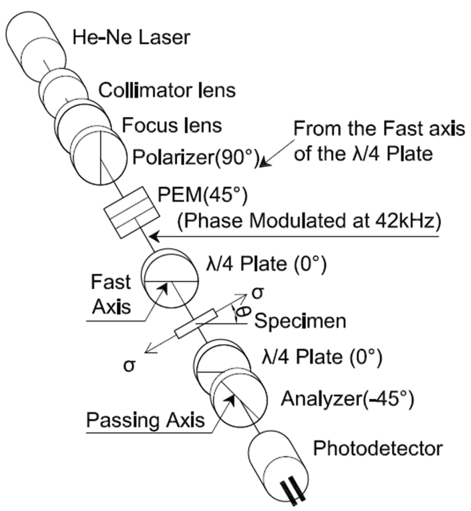
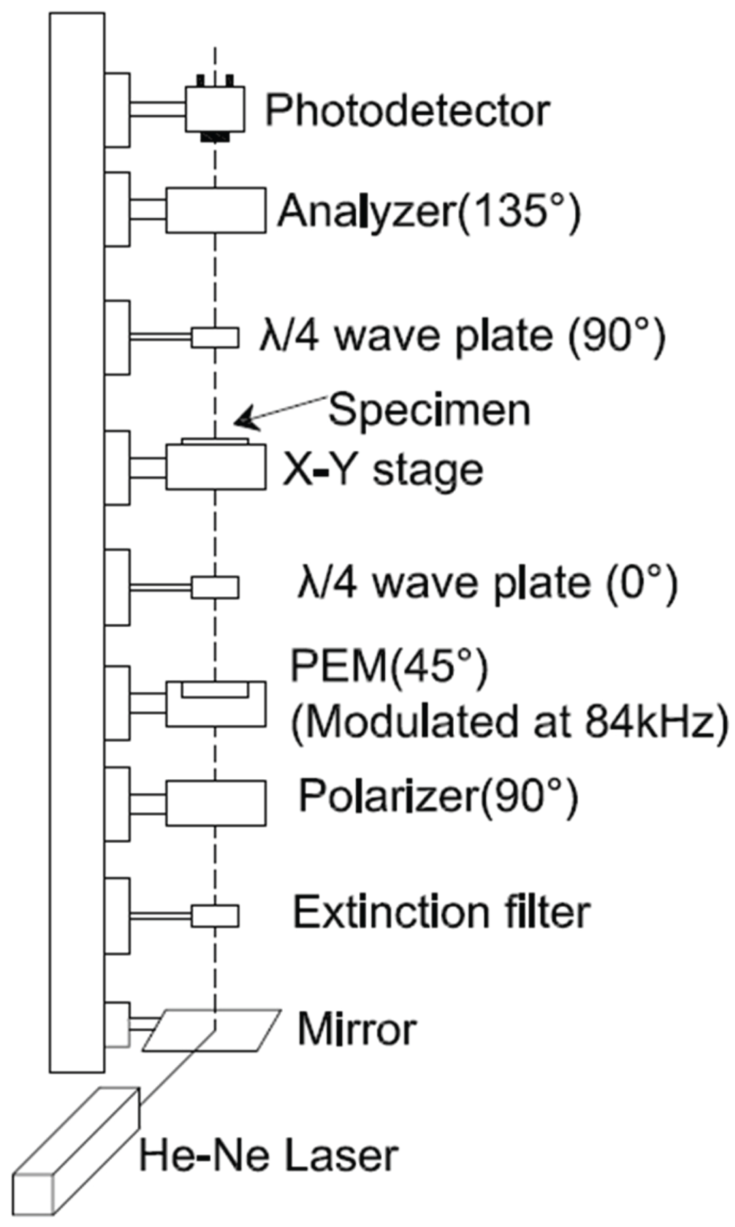
Figure 2: Optical alignments in reference....
Optical alignments in reference [6] (simplified version).
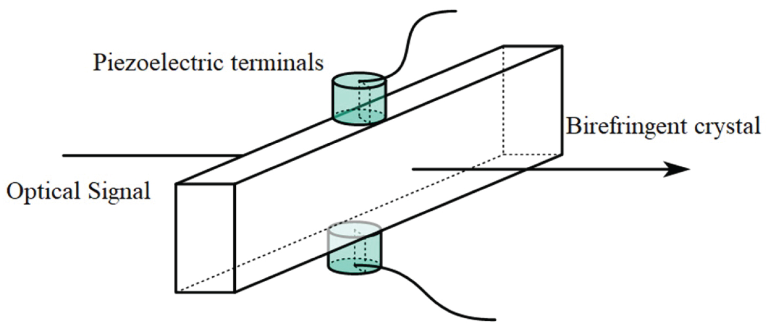
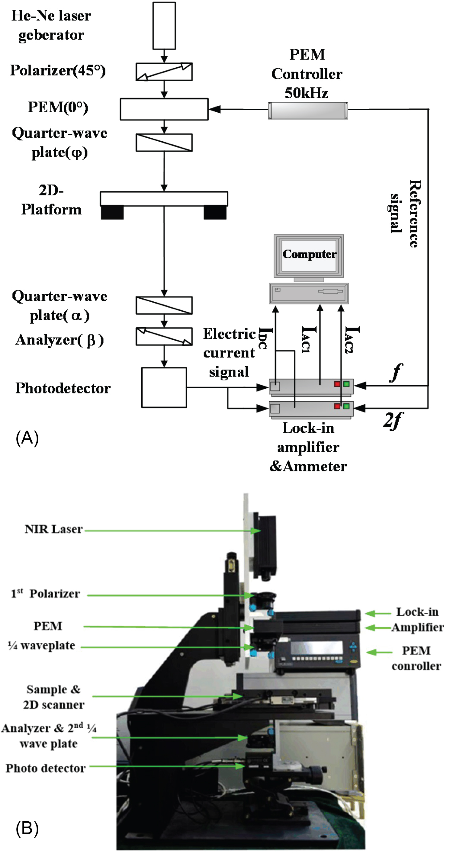
Figure 4: Schematic diagram of the optical....
Schematic diagram of the optical path (a) and experimental setup (b) used in the modulation method.
Tables
Table 1: The signs in Eq.(5) and Eq.(11) in different angle settings.
Table 2: The measurement errors due to misalignment of components.
References
- Fiorillo AS, Critello CD, Pullano AS (2018) Theory, technology and applications of piezoresistive sensors: A review. Sensors and Actuators A: Physical 281: 156-175.
- Gleskova H, Wagner S, Suo Z (1999) Failure resistance of amorphous silicon transistors under extreme in-plane strain. Applied Physics Letters 75: 3011-3013.
- He S (2005) Near infrared photoelasticity of polycrystalline silicon and it's relation to in-plane residual stresses. PhD thesis, Georgia Institute of Technology, Georgia.
- Wang B, Oakberg TC (1999) A new instrument for measuring both the magnitude and angle of low level linear birefringence. Review of Scientific Instruments 70: 3847-3854.
- Niitsu Y, Gomi K, Ichinose K (1997) Development of scanning stress measurement method using laser photoelasticity. JSME International Journal Ser A 40: 143-148.
- Gomi K, Ichinose K, Niitsu Y (2008) Residual stress estimation in SiC wafer using IR polariscope. International Conference on Electronic Materials and Packaging, IEEE, Taipei, Taiwan, 268-270.
- Hipps KW, Crosby GA (1979) Applications of the photoelastic modulator to polarization spectroscopy. J Phys Chem 10: 555-562.
- Theocaris PS, Gdoutos EE (2013) Matrix theory of photoelasticity. Springer.
- Goldstein DH (2016) Polarized light. CRC press, US.
- Gil JJ, Ossikovski R (2016) Polarized light and the Mueller matrix approach. (1st edn), CRC Press, US.
Author Details
Fei Su* and Bowen Zhang
School of Aeronautic Science and Engineering, Beihang University, Beijing, China
Corresponding author
Fei Su, School of Aeronautic Science and Engineering, Beihang University, Beijing, 100191, China.
Accepted: November 20, 2021 | Published Online: November 22, 2021
Citation: Su F, Zhang B (2021) Optical Alignments and Error Analysis of the Stress Measurement Technique Based on Photoelastic Modulator (PEM). Int J Opt Photonic Eng 6:042
Copyright: © 2021 Su F, et al. This is an open-access article distributed under the terms of the Creative Commons Attribution License, which permits unrestricted use, distribution, and reproduction in any medium, provided the original author and source are credited.
Abstract
A sensitive method for measuring the magnitude and angle of the fast axis of low level linear birefringence in optical materials has been developed over past 20 years. However, different optical alignments have been determined using the same data processing method. All possible optical alignments and their corresponding data processing are investigated in this paper to explore the mechanism of data processing. Proper applications of the system with different optical alignments are then suggested according to the investigation results. Furthermore, based on a specific optical alignment for low level birefringence measurement, quantitative error due to angle misalignment of optical components is evaluated, providing a guide to improve measurement accuracy.
Keywords
Photoelastic modulator, Low level birefringence, Optical alignment, Error analysis
Introduction
As the stress in wafer/chip has a significant influence on its thermal-mechanical reliability and electrical properties [1,2], it is important to measure the stress accurately. Compared with other non-destructive testing techniques such as micro-Raman spectroscopy, the infrared photoelastic method provides advantages of internal stress measurement and high measurement efficiency, as well as measurement results that are predominantly unaffected by temperature.
However, due to the weak photoelastic effect of silicon (with the typical stress optical coefficient at approximately 1.4 to 2.1 × 10⁻¹¹ [3]), the common infrared photoelastic method fails to meet standards of accuracy and sensitivity. To avoid such drawbacks, scholars [4-7] have employed the photoelastic modulator (PEM) to modulate the polarization state of the incident beam dynamically and periodically. After the beam passes through the specimen, its polarization state is further adjusted by specimen stress and the beam serves as an information carrier. The optical signal is then converted to an electrical signal using a photo detector in order to utilize the advanced facilities and knowledge which has accumulated in the field of electrical signal processing. Following this, the converted signal is input into a lock-in amplifier and the modulation frequency of PEM serves as the reference. The stress information, including phase retard and direction of principal stress, can be extracted from the carried signal with very high sensitivity using this technique.
Although a significant number of research papers have been published on this topic, the arrangement of optical components provided in these works are not unified. As examples, the optical alignments in reference [5] and [6] are provided in Figure 1 and Figure 2, respectively. While the core optical components and their arrangement sequence are exactly the same in both alignments, the relative orientations of optical axis of these components are different. In reference to the PEM, orientation of the polarizer, the 1st 1/4 wave plate and 2nd 1/4 wave plate and analyzer in these two alignments are 45°/-45°/-45°/-90° and 45°/-45°/45°/-90°, respectively, but their data processing is the same. As such, the principles informing the optical alignments and data processing are not conducive to providing comprehensive understanding or correct application of the method. To solve this problem, all feasible deploying methods of the system are provided in this work along with their respective applicable scenarios. A quantitative analysis of system error due to the misalignment of each component in the optical alignment is also provided.
Theoretical Basis of the Experimental Methods
In this paper, the Stokes vector is used to represent the optical information and the product transformation between the Muller matrixes [8-10] to illustrate the working principle of the system.
Working principle of PEM
The core of the PEM is a stress birefringent crystal that operates between two piezoelectric terminals. Under an excitation voltage signal with sine function shape (the excitation frequency is usually the natural frequency of the crystal), uniaxial stress with the same time period will be stimulated. For the polarized incident light, the crystal actually works as a phase retarder: , where is the phase difference coefficient of the PEM, depends on the highest voltage of the modulated signal, and can be adjusted through the PEM controller. Additionally, angular frequency and f is 50 kHz. The polarization state of the synthesized light after passing through the PEM is also periodic (Figure 3).
Optical setup and experimental principle
Optical setup with variable parameters: The optical path and corresponding experimental set up are shown in Figure 4, in which all angles are calculated based on the long edge of the PEM. The fast axis azimuth of the first quarter-wave plate or , fast axis azimuth of the second quarter-wave plate, and the polarization axis of the second polarizer are referred to as and ß respectively, and the direction of the principal stress and the phase retard at the incident point of the specimen is referred to as and , respectively. Thus, the variable parameters in this design are , and , and their relationships with the phase retard to be determined will be discussed. Non-linearity and hysteresis of PEM will be neglected, i.e., we assume that the performance of PEM is perfect.
Different alignments of the optical setup: According to the optical path setup and component arrangement in Figure 4, the final Stokes vector S' should be calculated according to:
Where is stokes vector of the incident laser beam, the and are the Muller matrix of the polarizer and analyzer, respectively, and their united expressions can be written as:
Where is the angle of polarization, for the first polarizer and for the second.
Additionally, M1 1/4, M2 1/4, Mspecimen and MPEM are the Muller matrix of the first and the second quarter wave plate, the specimen and the PEM, respectively. Their united expressions can be written as
Similarly, and are the optical axis orientation and phase retard of corresponding component, Specifically, or 45° and for the first 1/4 wave plate, and for the second one, , for PEM, and finally, both and are to be determined for specimen.
After matrix multiplying, the final expression of the light intensity I (which is the first component of the Stokes vector S') can be determined according to the following discussion:
A. In case the fast axis azimuth () of the first 1/4 wave plate is 0°
With the Fourier expansion of and , we have
In above equation, I0 is the initial light intensity of the laser source, K is the light transmittance of the whole system. J0、J1 and J2 are the 0th, 1st, and 2nd order of Bessel function, respectively. The meaning of α and β are denoted in Figure 1a.
When α and β match the value of any one of the eight settings in Table 1, the Eq (4) can be simplified to the following equation with only four items:
The three signs in above equation are related to the specific choice of α and β, and are summarized in Table 1.
An lock-in amplifier can be used to detect the DC term (IDC), the base-frequency term (IAC1) and the double-frequency term (IAC2) in Eq (5), we have:
By adjusting the PEM controller and setting δ0 = 2.405 such that, then
Where A1 and A2 are system parameters, which are not related to the wave length and the frequency of the PEM, and can be determined by calibration with the 1/4 or 1/8 wave plate. Until now, the phase retard δ of the specimen and the direction of the principle stress θ is denoted as:
As the δ is determined by cosine function, this optical alignment is sensitive to the variations of phase retard around 90°.
B. In case that the fast axis azimuth of the first 1/4 wave plate is -45° and +45° Similarly, when we have
For :
The only difference between Eq (9) and Eq (10) lies in the symbol before item.
By setting α and β to any of the values group shown in Table 1, Eq. (9) and Eq (10) can be simplified to:
Similarly, setting δ0 = 2.405 and using the aid of lock-in amplifier, provides:
Where B1 and B2 are also system parameters and can be calibrated with 1/4 or 1/8 wave plate. Phase retard (δ) and direction of the principle stress (θ) can then be determined using:
As the sine function is sensitive to around , this optical alignment is suitable to measure specimens with low phase retard like glass and silicon.
Theoretical Basis of the Experimental Methods
System error evaluation is performed taking the second optical alignment (i.e., , , ) as an example.
Using the assumption that each component in the system is correctly aligned and the parameters of PEM controller are set (i.e., wave length 1177 nm, ), the system is “calibrated” with an ideal 1/8 wave plate (which takes the place of the specimen) that works at near infrared red wave band. Referring to Eq. (12) (), after determining, , , and with the correct alignment, the theoretical coefficient of B1 can be determined as:
Similarly, the coefficient of B2 can be determined as:
Highly precise measurement of the system is based on the correct alignment of each optical component, however, misalignment of optical components may occur in which the optical axis of each component may not be set to their correct orientations. In this section, the measurement error of phase retard and direction of principal stress due to misalignment of the four components (i.e., the polarizer, the 1st and 2nd quarter wave plate, and the analyzer) in Figure 4 are thus evaluated.
Based on the second optical alignment, error evaluation is performed by keeping the other three optical components in their correct orientations, then each component is deviated from its orientation by up to 5° and the 1/8 wave plate used in the calibration is still employed as a specimen with fast axis aligned at 0°, 15° and 30°, 45°, respectively. Phase retard and direction of principal stress of the “specimen” is tested according to Eq. (13), enabling error evaluation of the system due to misalignment of each component, for example, the testing results of evaluation in a case in which the fast axis of the 1/8 wave plate is aligned at 15°, is summarized in Table 2.
By summarizing all these data, one can obtain the following conclusions:
1. Misalignment of the first 1/4 wave plate has the greatest influence on the measurement precision of the principal stress direction.
2. Misalignments of the first and second 1/4 wave plate have the same influence on the measurement precision of phase retard.
3. Misalignment of the analyzer has the greatest influence on the measurement precision of phase retard.
4. In cases that misalignments of all components are less than 5°, the maximum error of measured phase retard will be less than 10°.
5. Misalignment of the polarizer does not influence the measurement precision of principal stress direction.
Funding
National Natural Science Foundation of China under grant number 11672340.
Disclosure
The authors declare no conflicts of interest.