
International Journal of Optics and Photonic Engineering
(ISSN: 2631-5092)
Volume 8, Issue 1
Research Article
DOI: 10.35840/2631-5092/4555

Article Formats
Phase Control of Electromagnetic Wave by Double-Periodic Quasi Crystal Consisting of Nanoscale Semiconductor and Fullerene Layers
Table of Content
Figures
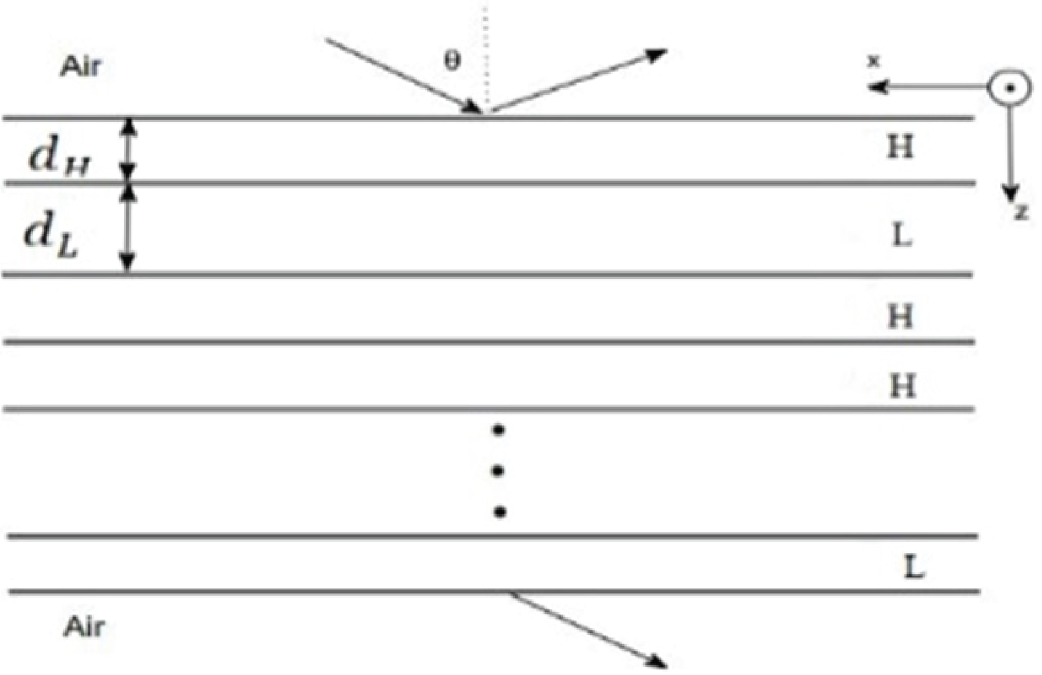
Figure 1: Schematic sketch of the...
Schematic sketch of the one-dimensional quasi-regular double-period structure, which is embedded in air. The thicknesses of H (fullerene) and L (Ge) are supposed to be dH and dL, respectively.
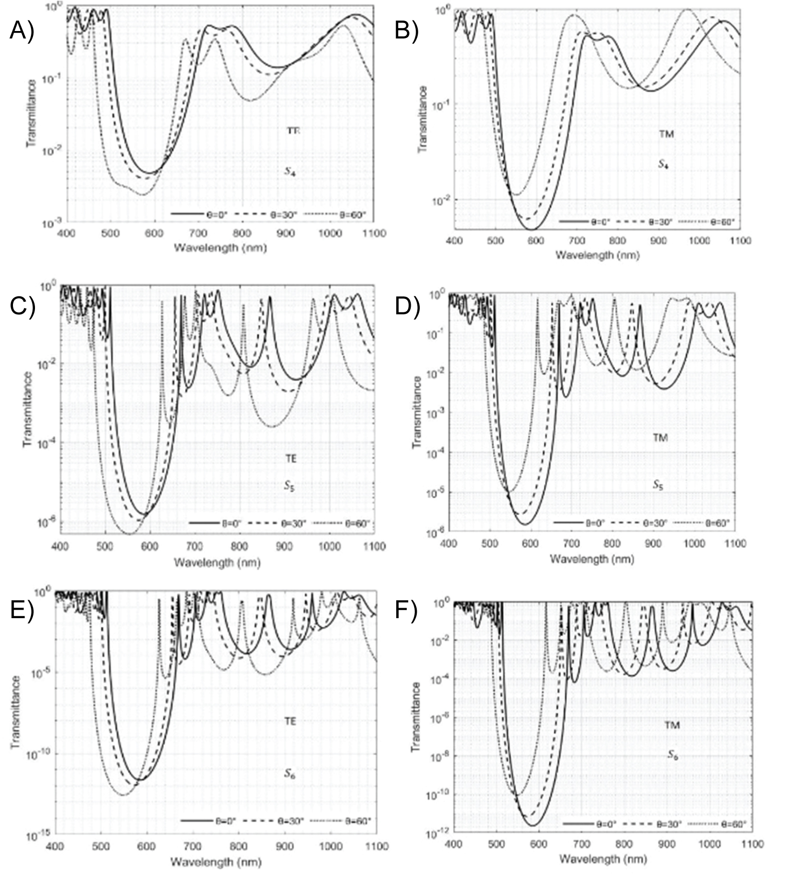
Figure 2: Transmission spectra of S4....
Transmission spectra of S4 S5 S6 fullerene and germanium double period quasiregular structure for TE and TM modes at a different angle of the incident as 0° (solid line), 30° (dashed line), and 60° (dotted line).
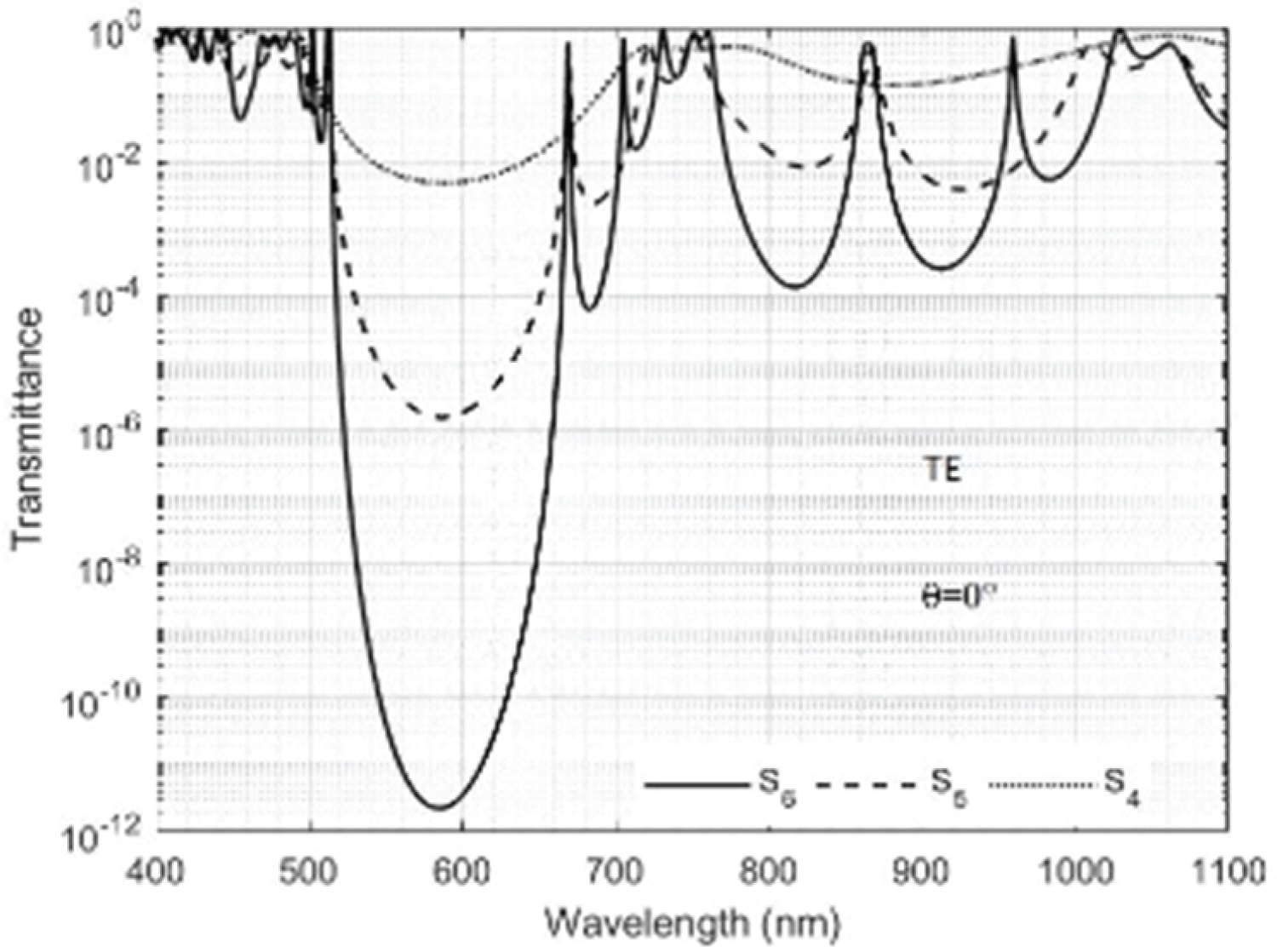
Figure 3: Calculated the transmission....
Calculated the transmission spectra of fullerene-germanium for three generations of double period orders as S6, S5, and S4 for TE mode at an angle of incident 0°. The physical characteristics match those of Figure 2.
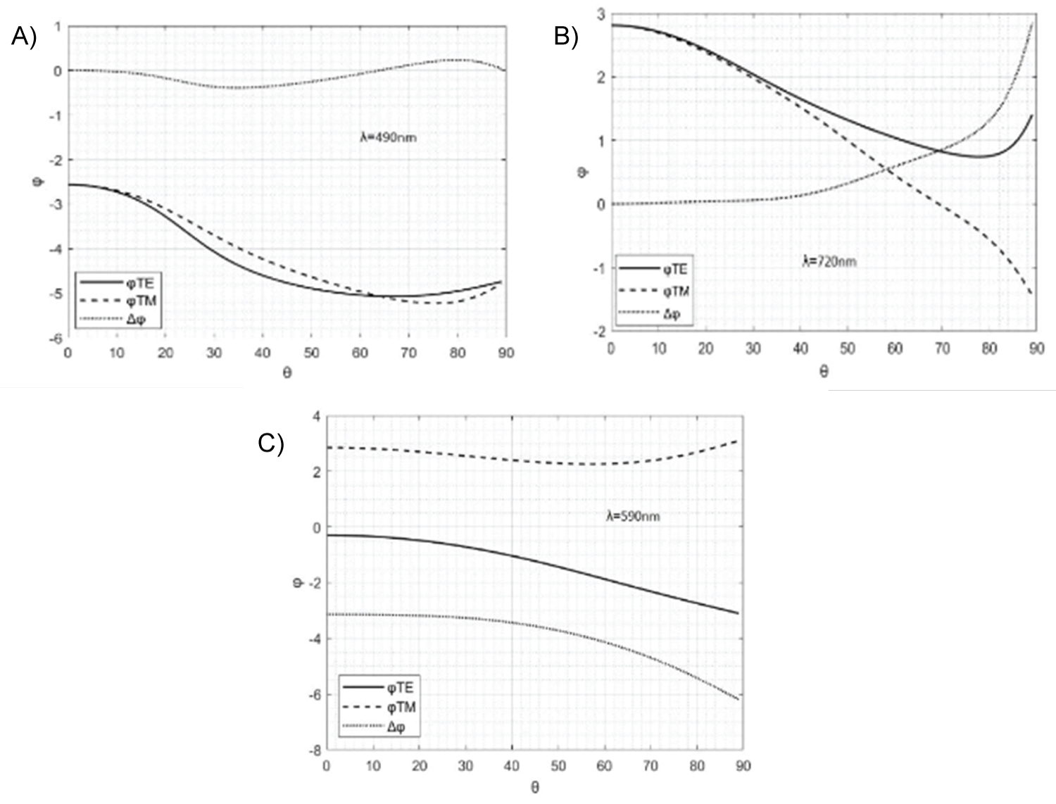
Figure 4: Calculated phase difference....
Calculated phase difference between the phase shift of TE and TM modes as a function of the angle of the incident in the stop band of fullerene-germanium multilayer structure, for the fourth generation of double period quasiperiodic structure.
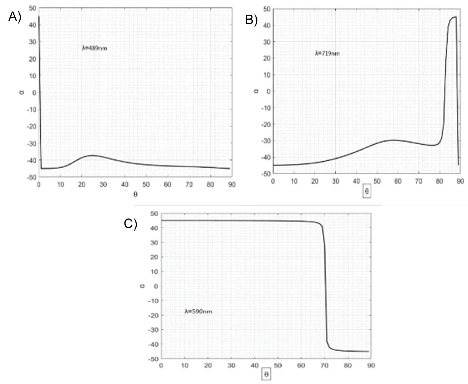
Figure 5: The tilt angle of transmission....
The tilt angle of transmission and reflection phases of the S4 DP sequence according to the angle of the incident with wavelength λ = 489 nm (lower edge), λ = 590 nm (center of gap), and λ = 719 nm (higher edge).
References
- Edrington AC, Urbas AM, DeRege P, Chen CX, Swager TM, et al. (2001) Polymer-based photonic crystals. Advanced Materials13: 421-425.
- Dadoenkova NN, Lyubchanskii MI, Shapovalov EA, Rasing TH (2003) Magnetic photonic crystals. J Phys D: Appl Phys36: R277.
- Joannopoulos JD, Villeneuve PR, Fan S (1997) Photonic crystals: Putting a new twist on the light. Nature 386: 143-149.
- Kurt B, Lölkes S, Wehrspohn RB, Föll H (2006) Photonic crystals: Advances in design, fabrication, and characterization. John Wiley & Sons.
- Zhu Q, Wang D, Zhang Y (2011) Control of photonic band gaps in one-dimensional photonic crystals. Optik 122: 330-332.
- Wu J-J, Gao J-X (2012) Transmission properties of Fibonacci quasi-periodic one-dimensional superconducting photonic crystals. Optik 123: 986-988.
- Rahimi H (2016) Analysis of photonic spectra in Thue-Morse, double-period and Rudin-Shapiro quasiregular structures made of high-temperature superconductors in the visible range. Optical Materials 57: 264-271.
- Shechtman D, Blech I, Gratias D, Cahn JW (1984) Metallic phase with long-range orientational order and no translational symmetry. Phys Rev Lett 53: 1951.
- Dov L, Steinhardt PJ (1986) Quasicrystals. I. definition and structure. Physical Review B 34: 596.
- Sahel S, Amri R, Gamra D, Lejeune M, Benlahsen M, et al. (2017) Effect of sequence built on photonic band gap properties of one-dimensional quasi-periodic photonic crystals: Application to Thue-Morse and double-period structures. Superlattices and Microstructures 111: 1-9.
- Walter S, Sutter-Widmer D (2007) Photonic and phononic quasicrystals. Journal of Physics D: Applied Physics 40: R229.
- Cheng YH, Chang CH, Chen CH, Hsueh WJ (2014) Bragg-like interference in one-dimensional double-period quasicrystals. Physical Review A 90: 023830.
- Kroto HW, Heath JR, O’Brien SC, Curl RF, Smalley RE (1985) C 60 : Buckminsterfullerene. Nature 318: 162-163.
- Akasaka T, Ando W, Kobayashi K, Nagase S (1993) Organosilicon derivatives of buckminsterfullerene (C60): First preparation of a fullerene silirane. Fullerenes, Nanotubes, and Carbon Nanostructures 1: 339-349.
- David WIF, Ibberson RM, Dennis TJS, Hare JP, Prassides K (1992) Structural phase transitions in the fullerene C60. EPL (Europhysics Letters) 18: 219-225.
- Karthik PS, Himaja AL, Singh SP (2014) Carbon-allotropes: Synthesis methods, applications, and future perspectives. Carbon Letters 15: 219-237.
- Hadi R (2015) Designing of tunable Quasi-regular photonic retarders made of Tellurium and C_ (60) fullerene subwavelength layers. Chinese Journal of Physics 53: 1-13.
- Gaevski ME, Kognovitskii SO, Konnikov SG, Nashchekin AV, Nesterov SI, et al. (2000) Two-dimensional photonic crystal fabrication using fullerene films. Nanotechnology 11: 270.
- Thompson RC (1990) Optical waves in layered media. 147-148.
- Srivastava SK, Ojha SP (2007) Omnidirectional reflection bands in one-dimensional photonic crystal structure using fullerene films. Progress in Electromagnetics Research 74: 181-194.
- Liu H, Wang J, Chanana A, Vardeny ZV (2019) Studies of spin transport in fullerene films. Journal of Applied Physics 125: 142908.
- Han P, Xu B, Liang J, Liu X, Bao H (2004) Band gaps of two-dimensional photonic crystal structure using fullerene films. Physica E: Low-dimensional Systems and Nanostructures 25: 29-34.
- Pedrotti FL, Pedrotti LM, Pedrotti LS (2017) Introduction to optics. (3 rd edn), Cambridge University Press.
Author Details
SS Khalid1,2* and SR Entezar2
1Physics Faculty, University of Tabriz, Tabriz, Iran
2Department of Physics, University of Halabja, Halabja, Iraq
Corresponding author
SS Khalid, Physics Faculty, University of Tabriz, Tabriz, Iran; Department of Physics, University of Halabja, Halabja, Iraq.
Accepted: April 27, 2023 | Published Online: April 29, 2023
Citation: Khalid SS, Entezar SR (2023) Phase Control of Electromagnetic Wave by Double-Periodic Quasi Crystal Consisting of Nanoscale Semiconductor and Fullerene Layers. Int J Opt Photonic Eng 8:055.
Copyright: © 2023 Khalid SS, et al. This is an open-access article distributed under the terms of the Creative Commons Attribution License, which permits unrestricted use, distribution, and reproduction in any medium, provided the original author and source are credited.
Abstract
This article studies the phase change of electromagnetic waves propagating in a quasi-periodic photonic crystal composed of fullerene and germanium nanolayers at the visible wavelengths. Since quasi-periodic crystals, like periodic structures, have band gaps that stop the propagation of electromagnetic waves, considering the geometry of ordering the layers we could identify the creation region of PBG for both TE and TM polarization waves, then we plotted the phase changes on both the center and the edges of our band gap when phase difference slowly changes. finally considering the electric field amplitude and our phase difference, it has been clear that when the passed light (elliptical polarization) is induced, a tilt angle is imaged according to the inducing angle. The method used in this article will be the famous transfer matrix method. Based on our findings, the proposed structure facilitates the construction of very compact phase controllers, including phase retarders and polarizers.
Keywords
Double period sequence, Quasiperiodic structure, Nano-scale fullerene, Phase controlling
Introduction
Photonic crystals (PCs) as periodic dielectric media have the potential to significantly advance our understanding of light manipulation and control [1]. Different materials with unique refractive indices are used to create the PCs in one, two, and three dimensions, respectively [2]. PCs may produce a photonic band gap (PBG) [3], which brings the idea of controlling the flow of light to the smallest level that the laws of physics allow [4]. Due to repeated Bragg scattering, electromagnetic waves of PBG frequencies cannot propagate through PCs. They have various applications, in optical switches, filters, waveguides, and photon polarization spectroscopy [5].
In recent decades, the optical properties of a new form of artificial crystal, the so-called quasi-regular multilayer structures, have also garnered considerable interest [6]. These structures, which are formed via a deterministic technique, show characteristics of periodic and random structures, and unique properties that do not exist in ordinary media [7]. Schechtman [8] and Levine and colleagues [9] provided experimental evidence for understanding these new classes of quasi-crystals. Recent examples of one-dimensional quasi-periodic (quasi-regular) structures include the Double periodic (DP) quasi-crystals [10]. More features of wave propagation in a DP quasi-crystal structure have been investigated by Steurer and Sutte [11], and Cheng, Y.H., and colleagues [12].
C60 buckminsterfullerene [13,14] is a group of compounds called fullerenes, which consist of a closed carbon cage, and has the highest stability [15]. Buckminsterfullerene is an enclosed spherical structure with hexagonal and pentagonal rings composed of carbon and designated as C60; the postfix indicates the number of carbon atoms in the formation, and each carbon atom is sp2 hybridization. There are about 12 pentagonal and 20 hexagonal rings [16]. By adjusting the geometry and degree of conjugation of the carbon superstructure, the electrical and optical characteristics of C60 fullerene films may be modified. This property of C60 fullerene can be used to make photonic crystal architectures with the help of fullerene films [17]. Fullerene (C60) in the form of a thin film structure is a viable choice for the creation of a PC structure due to its conductivity and near-zero absorption in the range of wavelength > 530 nm and approaching the infrared region [18].
The simplest example of a photonic crystal is the one-dimensional multilayer films. Fullerene (C60) has gained a great deal of scientific interest owing to its unusual optical and electrical characteristics and possible uses, such as alkali metal-doped C60 becoming a superconductor and doped thin films functioning as conductors [17]. Due to the easy modification of fullerene structure, the optical and electronic properties of fullerene films can be engineered by modifying the geometry and composition of the carbon superstructure. Having these properties, fullerene films could be good candidates for make photonic crystal structures. Thin layers of C60 have been grown on a number of metal and semiconductor substrates, such as GaAs [19], NiFe [20], Ge and Te [18], so forth and so on. This phenomenon is very important in both theory and practice, and it can be used in a wide range of new optical devices. Because more information about the details of how the fullerene films work as a PC could be important for the future development of its theory and use, it is important to find out more about these details [21].
In this study, the use of C60 fullerene/germanium (Ge) nano-scale multilayer sheets as 1D double periodic photonic quasiregular is looked into. Theoretically, the band characteristics, phase shift treatment, and polarization situation of electromagnetic waves in a 1D double periodic structure with nano-fullerene thin films are studied in depth for both TE and TM waves at different incident angles in the visible and near-infrared regions. To analysis the transmission characteristics of the presumed sub wavelength structure, we use the transfer matrix technique. This document is structured as follows: In Section 2, we describe the 1D layered structure using a mathematical model. In Section 3, the findings and comments are provided. The last section concludes the paper is Section 4.
Model and Numerical Techniques
There are basic deterministic laws that describe quasi-crystal photonic structures and cause them to form non-periodic and random patterns. The double period sequence is the prototypical case of non-periodic long-range order, and it can be generated deterministically by stacking two building blocks, L and H, in a certain order: given and for , with and , And the generating rule is executed repeatedly to produce: , etc. A geometrical arrangement of one-dimension, Figure 1 depicts the double-period multilayer construction that is implanted in the air. In this multilayer structure, layers L and H are anticipated to have thicknesses of d H and d L, respectively. Consequently, the H and L layers are regarded to be positive-index isotropic materials.
Consider a 1D quasiperiodic structure in the air composed of isotropic dielectric layers L and H stacked following the DP sequence along the z direction. We assume that the H layers are fullerene films with a refractive index of 2.1 and the L layers are germanium with a refractive index of 4.2. We use the transfer matrix technique to compute the transmission spectrum of the layered structure for an electromagnetic wave incident on the structure from the air at an angle θ. For transverse magnetic (TM) and transverse electric (TE) waves, it is assumed that the electric field E and magnetic field H are in the x direction (the dielectric layers are in the xy plane). We can show that the transfer matrix
Connects the tangential components of the electromagnetic fields at the beginning of the jth layer to those at the end of the layer [22]. Here, is the component of the wave vector along the z axis in jth layer, for transverse magnetic field (TM) wave, where is the permittivity of the vacuum, and for transverse electric field (TE) wave where is the permeability of vacuum, c is the speed of light in vacuum. The transmission coefficient may be written as
Here are the elements of the total transfer matrix which connects the tangential components of the electromagnetic fields at the beginning of the structure to those at the end of the structure.
Due to the phase and amplitude differences in the field transmitted by the ellipse, we infer that the light we apply to the structure is linearly polarized. To what extent does the ellipse's shape affect the angle it makes with the X-axis?
Thus, the solution to the tilt angle takes the form of the equation below
Where 𝜀 = Δφ = φTE-φTM, Take note that the amplitude ratio and phase difference can be used to rewrite this equation in a much more straightforward way [23].
Discussion and Results
In this section, we describe the numerical analysis of the suggested PC structures and demonstrate the transmission spectra and phase treatment of electromagnetic wave bands for both TE and TM-polarizations. At first, for the construction of our assumed structure, we consider fullerene-Ge arrangements. Here, all materials are assumed to be isotropic and absorb less. In the following numerical investigations, the refractive index nL = 2.1 and the thickness dL = 65 nm for L layers, for H layers the refractive index is nH = 4.2 and the thickness of H layers are dH = 40 nm, respectively. In this paper, the optical characteristics of quasiperiodic multilayer structures were calculated using the transfer matrix technique. Furthermore, we investigate the transmission spectra and phase treatment of electromagnetic waves in the situations listed above. For quasiperiodic structure DP generation numbers (S4 composed of 16 layers) (S5 composed 32 layers) and (S6 composed of 64 layers), respectively. For the 5th and 6th the number of layers L and H is different arrangements, the DP sequence for the 4th number of layers is L = 11 and H = 5 for the 5th number of layers L = 21 and H = 11, for the 6th (L = 43 and H = 21).
The Figure 2 shows transmittance spectra of 1D fullerene-germanium double period multilayer sequence for both TE (see Figure 1a, Figure 1c and Figure 1e and TM Figure 1b, Figure 1d and Figure 1f) polarizations versus visible- near-infrared wavelength range at different angles of the incident as 0° (solid line), 30° (dashed line) and 60° (dotted line). It is clear from these figures that in the transmission spectra C60-Ge there is a band gap for both TE and TM waves in the visible wavelength region nearly 490 nm to 720 nm, based on the same graph, as the angle of incidence increases for both TE and TM polarizations, the upper and lower sides of the gap shift to longer wavelengths.
Figure 3 presented a comparison between three generation double period quasiperiodic multilayers structure composed of fullerene - Ge nanolayers, the transmission spectra for TE polarization as the incident angle 0, for this purpose, the three-order double period sequence as S6 (solid line), S5 (dashed line), and S4 (dotted line). By considering the same physical parameters as that in Figure 2, it's clear, by increasing the order of the double period structure, the transmittance band remains invariant and the edges of the transmittance band become sharper. The transmittance band can occur in all higher-order double-period structures.
Now, what happens to phase difference in the higher, lower, and center of the band gap? Is it changeable? To answer this question, we consider the dependence of the phase difference between two TE and TM polarized transmitted waves in both edges of the gap and reflected waves in the center of the gap, the phase difference (Δφ = φTE-φTM) on the wavelength. Figure 4 depicts the phase difference between the phase shift of TE polarization and that of TM polarization as a function of the incidence angle in the stop band for the lower edge wavelength (see Figure 4a), the higher edge wavelength (see Figure 5b), and the central band wavelength (see Figure 5c). In addition, the fullerene- Ge arrangement has a lower band edge wavelength of = 490 nm, a central wavelength of = 590 nm, and a higher band edge wavelength of = 720 nm. Our calculations reveal that when the wavelength and incidence angle change, Δφ changes more slowly inside the stop band. As well as, at incidence angles close to = 0, the difference between the phase shifts of TE and TM waves is almost zero, insensitive to the incident angle; as the incident angle increases, the difference begins to change.
In the next figure, we clearly show the polarization properties of a one-dimensional Fullerene and Germanium double-period quasicrystal dielectric multilayer structure are had been investigated. We assume that we apply linearly polarized light to the structure, given the difference in phases and amplitudes of the field in which our polarization is transmitted in the ellipse. If the ellipse is shaped, what tilt angle does it make with the x-axis? We consider the two edges of the band gap and selected the first, last, and center wavelength bands, where the range of passage is greatest, the lower band edge wavelength λ = 489 nm, the higher band edge λ = 719 nm, and the center of the band is λ = 590 nm. Based on the above equation (see eq (2), the tilt angle α according to the angle of incident θ. Note that for all three low gaps, higher gap, and center gap, Consequently, the following inequality restricts the tilt angle of the elliptical of polarization: -45° < α < 45, the double period quasiperiodic multilayer structure of S4 generation observed from Figure 5a, Figure 5b and Figure 5c indicating that the linearly polarized incoming light has been changed to elliptic polarization. Polarization control and tuning are two of the most desirable possible uses of metal surfaces. Several key optical applications, including ellipsometry, polarimetry, optical sensing, and polarization-division multiplexing, rely on polarization manipulation for greater performance over conventional processes of material characterization and communication.
Conclusions
In this paper, the phase difference of waves that are reflected and transmitted in one-dimensional double-periodic crystals with nanoscale arrangements of fullerene and germanium has been studied using the transfer matrix method. For three different arrangements, it was found that the order of the double periods changed the band gap. So, we have completely shown that the layering geometry affects how a band gap is made. Similarly, as the angle of incident increases, the phase difference at the edges of the band gap will change more rapidly than in the center of the band gap, which changes more slowly. Because of the difference in the phases and amplitudes of our fields of reflection and transmission, our polarization became elliptical, resulting in an angle α with the x-axis. We expect that our research will aid in the study of the propagation characteristics and phase control of electromagnetic waves in quasi-periodic crystal formations, including metamaterials.
Acknowledgments
This work was supported by the ...