International Journal of Electronics and Device Physics
(ISSN: 2631-5041)
Volume 4, Issue 1
Research Article
DOI: 10.35840/2631-5041/1706
Compact Super-Directive Yagi-Uda Antenna Based on Parabolic-Shaped Reflector for Wireless Communications
AbdelRahman M Ghanim1*, Mohamed Hussein1,2, Rehab Hemdan1 and Ashraf Yahia1
Table of Content
- Abstract
- Keywords
- Introduction
- Simulation Methodology
- Results and Discussions
- The Optimized Design
- S-Parameter (S11)
- Radiation Efficiency
- Voltage Standing Wave Ratio (VSWR)
- Directivity
- Radiation Pattern
- Gain
- S-Parameter (S11)
- VSWR Parameter
- Comparing between the Simulated and Measured Results
- Conclusion
Figures
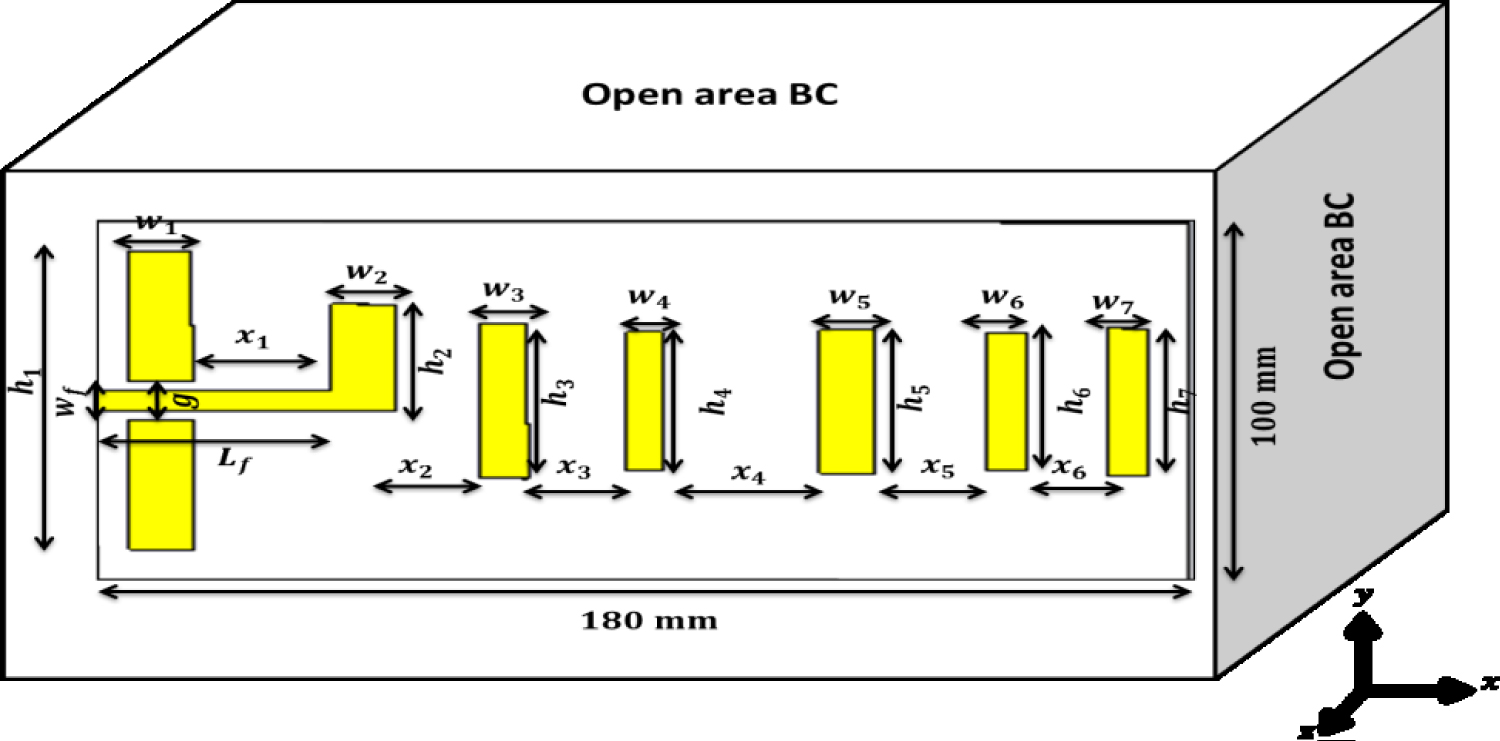
Figure 1: Three-dimensional computational domain....
Three-dimensional computational domain of the optimized microstrip Yagi-Uda antenna.
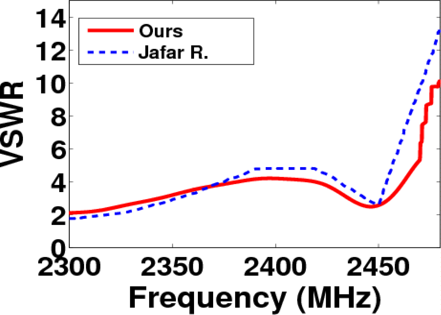
Figure 2: Variations of the calculated VSWR by.....
Variations of the calculated VSWR by FIT method compared with the results published by Jafar R [14].

Figure 4: The reflection coefficient (S11) as a....
The reflection coefficient (S11) as a function of the frequency of the optimized design with curved reflector, the optimized design and Jafar R [14].
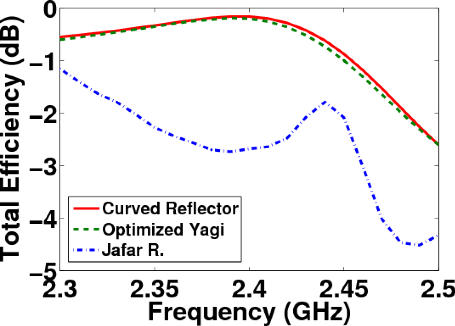
Figure 5: Frequency dependent radiation efficiency....
Frequency dependent radiation efficiency of the optimized design with curved reflector, the optimized design and Jafar R [14].
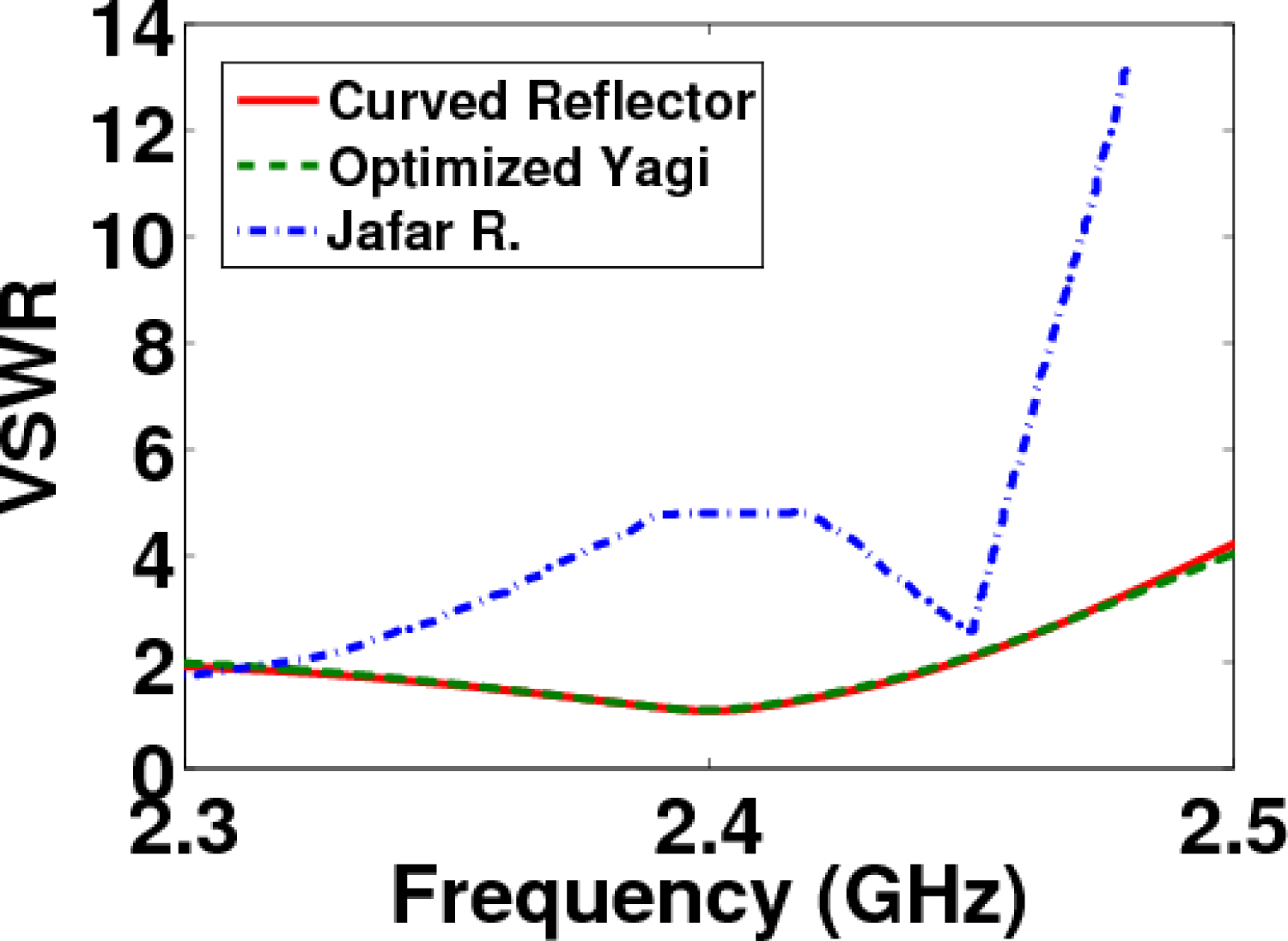
Figure 6: VSWR as a function of the frequency....
VSWR as a function of the frequency for the optimized design with curved reflector, the optimized design and Jafar R [14].
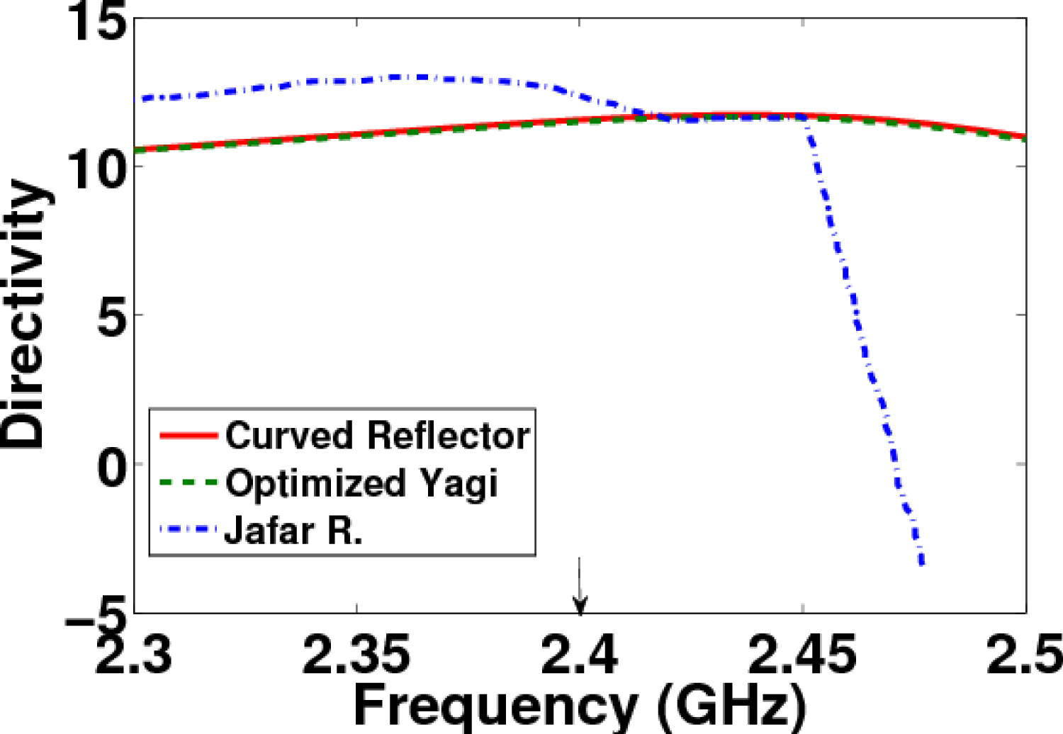
Figure 7: Variation of the directivity with frequency...
Variation of the directivity with frequency for the optimized design with curved reflector, the optimized design and Jafar R [9].
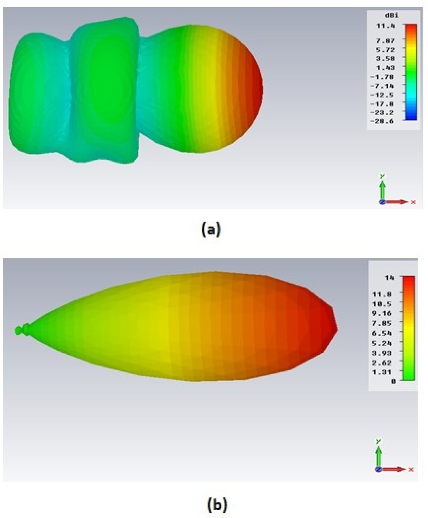
Figure 8: Radiation Pattern of the optimized design with...
Radiation Pattern of the optimized design with curved reflector at 2.4 GHz with: (a dB scaling and; (b Linear scaling.

Figure 9: Variation of gain with frequency for the optimized ...
Variation of gain with frequency for the optimized design, the optimized design with curved reflector and Jafar R [14].
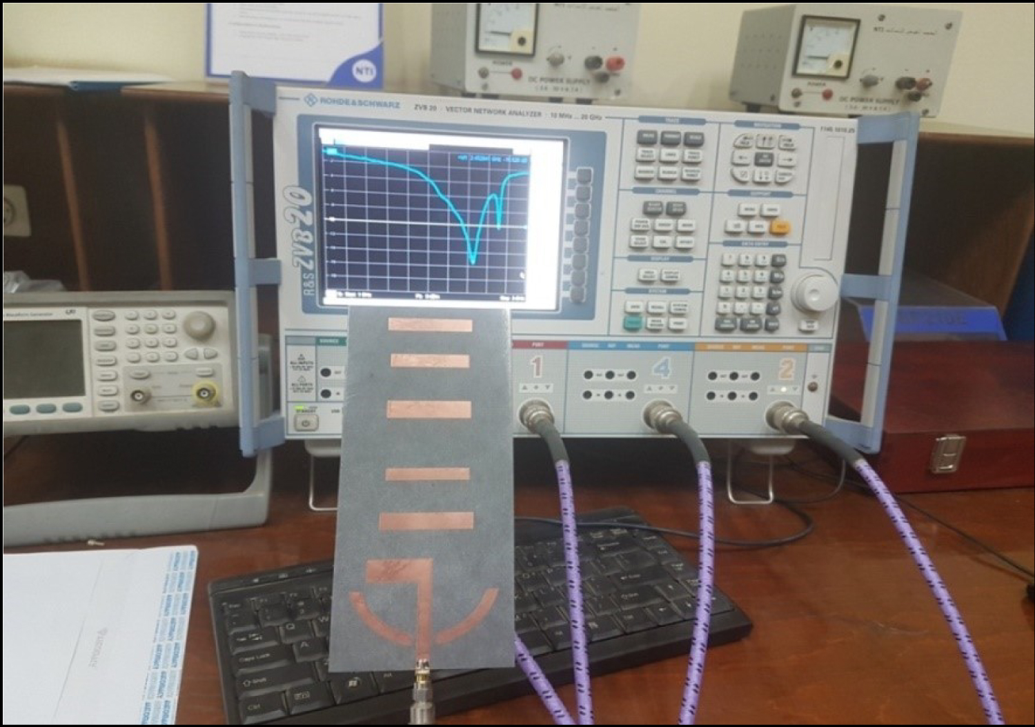
Figure 11: The spectrum analyzer connected with...
The spectrum analyzer connected with the Yagi design.
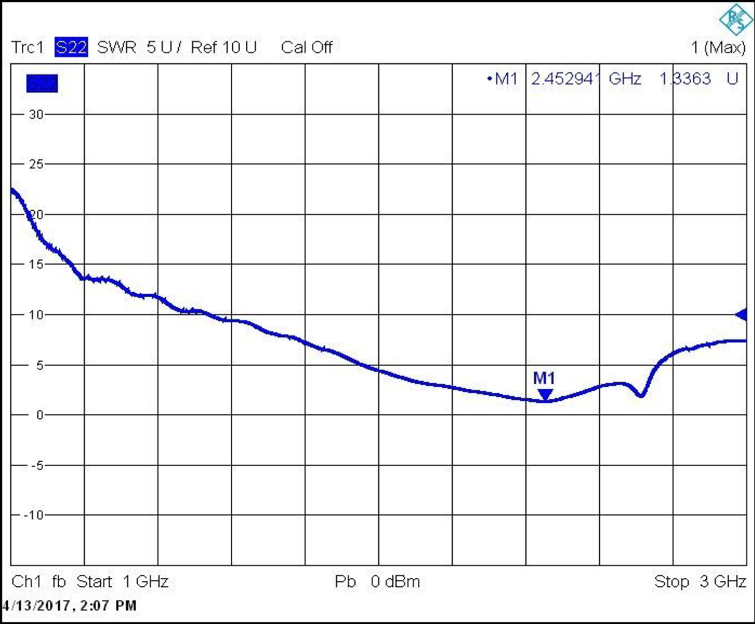
Figure 13: The VSWR measurement for the fabricated....
The VSWR measurement for the fabricated design.
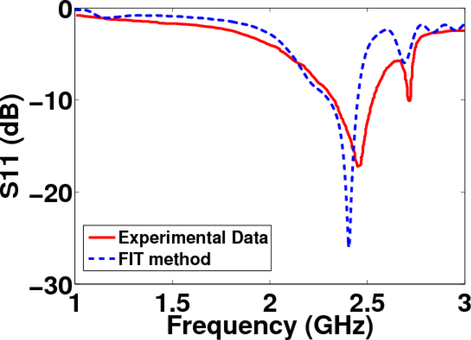
Figure 14: Simulated and measured reflection coefficients...
Simulated and measured reflection coefficients versus the frequency range.
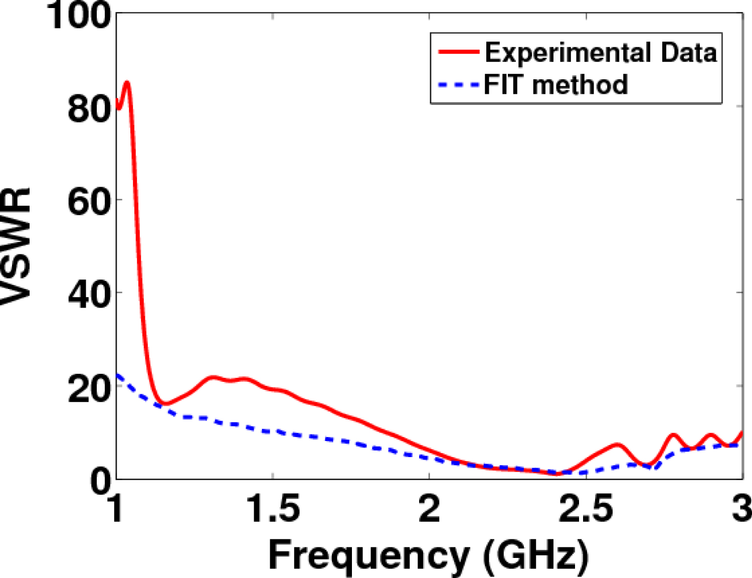
Figure 15: Simulated and measured VSWR plotted as a....
Simulated and measured VSWR plotted as a function of frequency.
References
- Yeo CL (2000) Active microstrip array antennas. The School of Computer Science and Electrical Engineering, University of Queensland. Submitted for the degree of Bachelor of Engineering (Honours) in the division of Electrical and Electronic Engineering.
- Khattak MK, Siddique O, Ahmed W (2011) Design and simulation of microstrip phase array antenna using ADS.
- Garg R, Bhartia P, Bahl IJ, Ittipiboon A (2001) Microstrip antenna design handbook: Artech house.
- Sun BH, Zhou SG, Wei YF, Liu QZ (2010) Modified two-element Yagi-Uda antenna with tunable beams. Progress In Electromagnetics Research 100: 175-187.
- Liang CH, Cheng D (1983) Directivity optimization for Yagi-Uda arrays of shaped dipoles. IEEE Transactions on Antennas and Propagation 31: 522-525.
- Balanis CA (2016) Antenna theory: Analysis and design. (4th edn), John Wiley & Sons, US.
- Stutzman WL, Thiele GA (2012) Antenna theory and design. John Wiley & Sons.
- Kishore VK, Nalini K, Madhav BTP, Raj Gopala Rao BV, Surendra Kumar B, et al. (2011) Design and analysis of 3-Element Yagi-Uda antenna for wind profiling radar. International Journal of Computer Science & Communication Networks 1: 242-246.
- Sharma G, Anand NS, Ashish D, Singhal PK (2012) Yagi-Uda antenna for L-band frequency range. International Journal of Engineering & Technology 1: 315-320.
- Stutzman W (2008) Bibliography for antennas: A list of every English-language antenna book ever written. IEEE Antennas and Propagation Magazine 50: 128-143.
- Alhalabi RA, Rebeiz GM (2009) High-gain Yagi-Uda antennas for millimeter-wave switched-beam systems. IEEE Transactions on Antennas and Propagation 57: 3672-3676.
- Goshwe N, Tijam I (2012) Optimal design of Yagi-Udi antenna for VHF band application using magus 2.2 software. Am J Sci Ind Res 3: 277-282.
- Floc'h JM, Ahmad AES (2013) Broadband quasi-yagi antenna for wifi and wimax applications. Wireless Engineering and Technology 4: 87-91.
- Mohammed JR (2013) Design of printed yagi antenna with additional driven element for WLAN applications. Progress In Electromagnetics Research C 37: 67-81.
- Abdullah Alshahrani KA, Falah A, Khloud A (2015) Designing and building a Yagi-Uda antenna array. International Journal of Multidisciplinary Research and Development 2: 296-301.
- Yeo J, Lee JI (2017) Design of tri-band double-dipole quasi-yagi antenna using dual co-directional SRRs. Microwave and Optical Technology Letters 59: 1354-1357.
- Ghanim AM, Rimal HP, Cutugno F (2019) Dynamic losses prediction in NOG electrical steels for electrical machines. In 2019 IEEE (5th edn) International forum on Research and Technology for Society and Industry (RTSI) IEEE.
- Antonio SQ, LoZito GM, AbdelRahman MG, Laudani A, Rimal H, et al. (2020) Analytical formulation to estimate the dynamic energy loss in electrical steels: Effectiveness and limitations. Physica B: Condensed Matter 579: 411899.
- Ghanim AM, Mohamed H, Mohamed Farhat OH, Ashraf Y, Salah SAO (2018) Design considerations of super-directive nanoantennas for core-shell nanowires. JOSA B 35: 182-188.
- Ghanim AM, Mohamed H, Mohamed Farhat OH, Ashraf Y, Salah SAO, et al. (2016) Highly directive hybrid Yagi-Uda nanoantenna for radition emission enhancement. IEEE Photonics Journal 8: 1-12.
- Cai B, Sun L, Lei Y (2019) 3D printing using a 60 GHz millimeter wave segmented parabolic reflective curved antenna. Electronics 8: 203.
Author Details
AbdelRahman M Ghanim1*, Mohamed Hussein1,2, Rehab Hemdan1 and Ashraf Yahia1
1Physics Department, Ain Shams University, Egypt
2Centre for Photonics and Smart Materials, Zewail City of Science and Technology, Egypt
Corresponding author
AbdelRahman M Ghanim, Physics Department, Ain Shams University, 11566, Cairo, Egypt, Tel: (+39)-333-779-3922.
Accepted: August 17, 2020 | Published Online: August 19, 2020
Citation: Ghanim AM, Hussein M, Hemdan R, Yahia A (2020) Compact Super-Directive Yagi-Uda Antenna Based on Parabolic-Shaped Reflector for Wireless Communications. Int J Electron Device Phys 4:006
Copyright: © 2020 Ghanim AM, et al. This is an open-access article distributed under the terms of the Creative Commons Attribution License, which permits unrestricted use, distribution, and reproduction in any medium, provided the original author and source are credited.
Abstract
This paper was undertaken to study the influence upon gain and directional characteristics caused by numerous array of elements when used in conjunction with the Yagi antenna. Antennas are beneficial for a wide range of applications such as point to point communication, radio broadcasting, radar, and wireless LAN. However, maximum gain and maximum directivity with low losses are the desired characteristics that are sought. In this paper, the novel design of ultra-directive microstrip Yagi design (frequency = 2.4 GHz) is simulated and analyzed. We used the FIT technique to obtain the optimized parameters (geometrical parameters) for the Yagi design. Also, the antenna parameters (gain and directivity), and the matching parameters (VSWR and S11) are simulated using the finite integral technique (FIT). The proposed design showed high directivity and high gain with a narrow beam. Additionally, the investigated design exhibits low loss power due to the low value of the backscattering and also S11 value. The measured results for the matched parameters of the investigated design are taken from the network analyzer. For our proposed design, the experimental results are very close to the simulated results. The suggested Yagi antenna design may be beneficial for many applications including, Wi-Fi, Bluetooth applications, and wireless applications.
Keywords
Yagi-Uda, Directivity, Finite integration technique, Radiation pattern
Introduction
Communication can be generally defined as the transfer of information from point to point [1]. The use of the communication system is usually when the information is to be sent over a distance [1,2]. In today's spacecraft and aircraft applications where the antenna's size, cost, weight, performance, ease of installation, and fabrication profile are of utmost consideration [2]. The low-profile microstrip antenna is widely used over conventional antenna [3]. One of the most popular and widely used antennas is the printed Yagi-Uda antenna because of its, low cost, simplicity, highly directional radiation, and relatively high gain [4].
The printed Yagi-Uda antenna arrays widely used in important applications in the very high frequency/ultrahigh-frequency (VHF/UHF) range like home TV applications and modern wireless communications [5]. The Yagi-Uda array is the arrangement of a row of straight cylindrical conductors, of which only one is driven (source) and all the others are parasitic [4,5]. The parasitic elements normally consist of several reflectors and directors that enhance the radiation in the desired direction when well arranged on a supporting structure [6,7]. The spacing and length of the reflector affect the forward gain and have a large effect on the backward gain (F/B ratio) as well as the input impedance (Zin). Consequently, it can be used to optimize and control antenna parameters [8]. The spacing and length of the directors have large effects on the forward radiation, backward radiation ratio, and the input impedance [6]. They are considered to be the most effective elements of the array [9].
The parasitic elements are attached close to the driven element and are not connected directly to the source [10]. Instead, induced currents are generated in the parasitic elements due to the radiation field of the driven element causing them to radiate in turn [6]. To enhance the directivity of the Yagi antenna, the length and the position of the elements have to be optimized to produce constructive radiation in one direction. The phase of the currents flowing in the additional elements of the antenna is the key element to the Yagi-Uda theory [11]. The parasitic elements of the Yagi-Uda antenna operate by re-emitting their signals in a slightly altered phase to that of the feed element [12].
Recently, several works have been directed towards the far-field region enhancement. In 2010, A modified two-element Yagi-Uda antenna [4] with tunable beams in the H-plane (including four significant beams: forward, backward, Omni-directional, and bi-directional beams) was presented [4]. A two-element array with L1 = 0.46 λ, L2 = 0.38 λ, S = 0.25 λ, D = 0.028 λ, λ = 850 MHz and a = b = d = 0:0029 λ is analyzed [4]. The maximum gain for the antenna design reaches 5.3 dB with VSWR ≤ 2 [4]. In 2013, Floc'h, et al. [13] presented a broadband quasi-Yagi antenna. Good impedance matching is obtained by using parasitic elements [13]. The antenna has been designed and successfully measured. Experimental results show that the 10-dB return loss bandwidth of this antenna is 50% operating from 2.3 GHz to 3.8 GHz. A very flat gain is obtained (around 5 dB) over the entire bandwidth [13]. In the same year, a new configuration of the Yagi antenna was proposed, which improved the forward/backward ratio (F/B) significantly while maintaining a high gain [14]. This configuration involves the addition of one radiating element to the original Yagi array. The numerical and measured results of this design showed more than 20 dB front to back ratio at 2.4 GHz [14]. Two years later, Antennas were introduced in general than one type of the antenna was been focused on which was the Yagi-Uda [15]. Also, the process of designing a four-element Yagi-Uda antenna that consists of one driven element, one reflector, and two directors was introduced [15]. It has been shown that the resonant frequency is slightly over 2.5 GHz and with a resonant magnitude of -35 dB with directivity of 5.124 dB [15]. In 2017, a tri-band double dipole quasi-Yagi antenna (DDQYA) using dual co-directional split-ring resonator (SRRs) was proposed [16]. The measured frequency bands were 1.224-1.231 GHz, 1.563-1.608 GHz, and 1.65-2.88 GHz, respectively, which in agreement well with the simulated ones [16]. The measured peak gain was 1.9-2.5 dB in the first band, whereas it was 5.9-6.7 dB in the second. In the 1.7-2.6 GHz band, the gain was 6.3-6.9 dB [16].
Several wireless local area networks (WLAN) applications use omnidirectional antennas [1]. However, the directional antennas such as patch Yagi arrays have been engaged to reduce the unwanted radiofrequency radiations in addition to the unwanted interference in other directions. Patch Yagi antennas have been operated in scientific, industrial, and medical (ISM) applications at 2.4 GHz where the high directional emission is necessary for point-to-point communications and long- distance wireless communications. In this paper, seven elements printed Yagi antenna has been investigated and analyzed using a numerical electromagnetic technique called the finite integration technique (FIT method) [17,18]. The proposed design showed high directivity and a high gain of 12 dB at the frequency range of 2.4 GHz. The antenna parameters have been optimized to obtain good matching with the transmission line. The optimized design has been fabricated using the photolithographic method and a good agreement is shown between the measured and the simulated results.
Simulation Methodology
The investigated Microstrip Yagi-Uda antenna shown in Figure 1 consists of seven elements (driven element, one reflector, and five directors). The length of the dipole element (source) is equal to h2 connected with a reflector of length h1 with gap g to re-radiate the backward radiation to the specific direction. Furthermore, five directors have been used with different lengths as follows: h3, h4, h5, h6, h7 from the first to the fifth director, respectively. However, the widths of the reflector, the dipole, and the five directors are w1, w2, w3, w4, w5, w6, and w7, respectively. Also, the width of the feed patch is equal to wf with a length of Lf. Further, the distance between the reflector and dipole element is equal to x1 and the distance between the dipole and the first director is x2. Additionally, the distances between the directors are x3, x4, x5, and x6. The substrate material is Rogers RT5880 with thickness 1.57 mm, width 100 mm and 180 mm in length.
The proposed design of the microstrip antenna is simulated using electromagnetic 3-D finite integration technique (3-D FIT) via computer simulation technology (CST MWS) software package. Figure 1 shows the 3-D computational domain for the simulated unit cell of the proposed Yagi-Uda design. The unit cell is surrounded by air as an open area boundary conditions (BCs) along with the x, y and z directions to give extra distances for the far field calculations. In this study, the microstrip Yagi design is excited by the feed element that consists of a waveguide port connected with the driven element. The directivity and the radiation efficiency of the Yagi antenna are used as a figure of merit to study the performance of the proposed design. The directivity of the propagating radiation is defined as:
Where is the radiated power per unit solid angle in the desired direction, divided by the power radiated per solid angle in all directions. The radiation efficiency quantifies the electrical losses occur throughout the antenna and it is defined as:
Where and are radiated and loss powers, respectively.
Results and Discussions
Numerical results
To validate the simulation results, the Microstrip Yagi design is initially simulated using the 3D-FIT method and compared with published results carried out by Jafar R. [14]. In this investigation, the microstrip Yagi antenna consists of seven dipoles (one reflector, one radiating dipole, and five directors). Their lengths and x-locations were in units of λ (λ = 12.4 cm) [14].
h = [h1, h2, h3, h4, h5, h6, h7]
= [0.51 λ, 0.490 λ, 0.430 λ, 0.430 λ, 0.430 λ, 0.430 λ, 0.430 λ] [14].
x = [x 1, x 2, x 3, x 4, x 5, x 6, x 7]
= [-0.25 λ, 0, 0.31 λ, 0.62 λ, 0.93 λ, 1.24 λ, 1.55 λ] [14].
Figure 2 shows VSWR as a function of the frequency calculated by the 3D-FIT method and those obtained by [14]. A good agreement is revealed from the figure between the 3D-FIT results and the published results [14].
The Optimized Design
It is aimed to tune the geometrical parameters of the microstrip Yagi design reported in [14]. The microstrip Yagi antenna, shown in Figure 1, consists of the driven element, the directors, and the reflector [4]. The reflector, the director, and driver of the antenna are located on the plane with the same high dielectric substrate so that the surface waves produced by the antenna are focused on the end-fire direction. This antenna design is in the sense that reflector on the back of the driven element is utilized to emit back the radiation from the backside to the forward direction [19]. In other words, the reflector element helps to diminish the surface wave traveling to the backside direction. The unique design of the Yagi antenna results in an antenna with relatively high directivity, high gain, and wide bandwidth. The microstrip-Yagi antenna keeps both compactnesses of resonant-type antennas along with broadband characteristics of traveling-wave radiators. The compact and simple design is compatible with any microstrip-based MMIC circuitry. The antenna can be fabricated easier due to its uniplanar nature.
The optimized yagi antenna consists of seven elements (one dipole, one reflector, and five directors) as shown in Figure 1. The geometrical parameters of the proposed Yagi antenna are listed in Table 1. The length of the dipole element is expected to satisfy the resonance condition. The used substrate material is Rogers RT5880 with thickness 1.57 mm and the copper thickness is 0.035 mm. By the aid of optimization design, the length of the proposed antenna is reduced to 180 mm as compared with 300 mm of the previous work [14]. The optimized Yagi design is simulated over the range from 2.3 GHz to 2.5 GHz with a resonance frequency at 2.4 GHz.
To enhance the performance of the proposed design, the geometrical parameters of the investigated microstrip Yagi-Uda antenna have been analyzed thoroughly. The influence of the space between the feed element and the passive elements (reflector and directors) is primarily considered. The space between the dipole source and the passive elements increases the undeniable coupling effect [20]. A suitable distance between the reflector and the dipole source increases the directivity of the antenna due to the accompanying decrease in the backward radiation lobes as shown in Table 1. On the other hand, the length of the reflector influences the forward gain but has a large effect on the backscattering gain (F/B ratio). The dipole length has little effect on the forward radiation but a large effect on the backward radiation. The length of the directors has large effects on the forward emission and backward gain ratio as will be explained later Table 2.
The optimized design with curved reflector
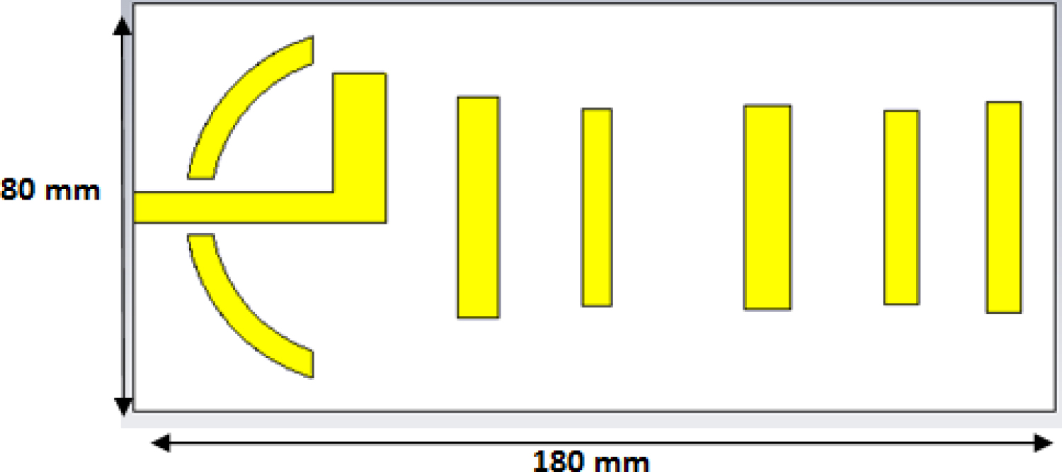
The main function of the reflector element in the Yagi antenna design is to reflect the backward radiation to the specific direction of propagation. The reflector is the element that is placed at the rear of the driven element (The dipole). Its resonant frequency is lower, and its length is approximately 5% longer than the driven element. Its length will vary depending on the spacing and the element diameter. The spacing of the reflector is between 0.1 λ and 0.25 λ. Its spacing depends upon the gain, bandwidth forward to backward ratio, and sidelobe pattern requirements of the final antenna design. In this work, we have used the curved reflector to optimize the gain of the microstrip Yagi design and enhance the directivity and s11. Besides, the substrate width of the Yagi design is decreased and reached 80 mm as compared with the optimized design of 100 mm as shown in Figure 3. The geometrical parameters of the optimized design with curved reflector are the same as the optimized design except for the reflector with a length of 67 mm.
The parabolic reflector shown in Figure 3 affects the antenna performance by obscuring the reflected parallel electromagnetic waves because of the size of the feed at the parabolic focus. As the name suggests, the parabolic element is formed from a shape called a paraboloid. The parabolic reflector theory depends on the shape of the reflector for its properties [21]. The reflector element uses a parabolic shape to certify that all the radiated power is reradiated in a beam in which the wave traces run parallel to each other. Additionally, the entire reflected power is all in phase, due to the path length from the reflector to the source, and then outwards is equal wherever it is reflected on the surface of the parabola. In other words, this shape forms the reflective surface in the antenna that enables waves reradiated back by the surface to keep their phase relationship, thus enabling the maximum gain to be achieved [21]. The parabolic reflector will reflect the traveling RF plane wavefront comes towards the antenna and remain in phase at the focal point. In this way, the entire signal remains in phase without any cancellation. This means that the maximum wave is conserved.
S-Parameter (S11)
As we have used only one probe feed in our design, we will find only the input reflection coefficients or the s-parameter of the optimized Yagi design. The simulation results of the optimized design are shown in Figure 4.
Figure 4 gives us clear information about the performance of our design. In Figure 4 we can see that the designed antenna resonates at the desired frequency which is 2.4 GHz. At the resonant frequency, the input reflection coefficient has the minimum magnitude which is about -28 dB. In Figure 4, the input reflection coefficient (s11) for the optimized design (dotted green line) is about -26 dB and the optimized design with curved reflector is about -28 dB (solid red line). The s11 for the optimized design with a curved reflector is enhanced as compared with the previous work [14] of -9 dB (dotted blue line) with an enhancement of 85%.
Radiation Efficiency
The antenna efficiency takes into account the reflection, conduction, and dielectric losses. The conduction and dielectric losses of an antenna are very difficult to compute and in most cases, they are measured. Even with measurements, they are difficult to separate and they are usually lumped together to form the ecd efficiency. The resistance RL loss is used to represent the conduction-dielectric. The conduction-dielectric efficiency ecd is defined as the ratio of the power delivered to the radiation resistance Rr the power delivered to Rr and RL. The radiation efficiency can be written as [6]:
The efficiency of this antenna is shown in Figure 5. The efficiency of optimized design with a curved reflector is far better than the efficiency of the work presented by Jafar R [14]. The efficiency of the optimized design is -0.5 dB while the radiation efficiency for the optimized design with curved reflector is about -0.3 dB at 2.4 GHz. The antenna efficiency for the design introduced by Jafar R [14] is about -2.5 dB which is far less than our design.
Voltage Standing Wave Ratio (VSWR)
The ratio of maximum to minimum values of voltage is called the voltage Standing wave ratio (VSWR) [6]. Therefore,
Since for a passive load, the minimum value of the VSWR will be unity (for a matched load) while its maximum value can be infinity (for total reflection, with a short circuit or an open circuit as the load). Figure 6 shows the comparison between the VSWR results for the optimized design, the optimized design with curved reflector, and the design presented by Jafar R [14]. It can be noted from this figure that our design showed good matching as compared with the previous work. The VSWR for the optimized design is 1.5 and the optimized design with curved reflector is 1.3 at 2.4 GHz. While the VSWR for the previous work [14] is 5 < 2 at 2.4 GHz which showed very bad matching of the antenna design with the transmission line.
Directivity
The directivity of the antenna is the ratio of the maximum radiation intensity to the average radiation intensity [6]. The average radiation intensity is equal to the total power radiated by the antenna divided by 4π. The directivity of the antenna design presented by Jafar R [14] is high and its value is about 12 dB. Figure 7 shows the directivity of the optimized design, the optimized design with cured reflector and Jafar R [14]. It can be seen from this figure that the directivity of our design kept the same as Jafar R design with a value of about 12 dB. Additionally, the directivity of our design is still constant over the range from 2.3 GHz to 2.4 GHz which is better than the previous work. When the frequency reached 2.45 GHz, The directivity of the previous work showed fast decay from 12 to zero other than our design which kept constant over the frequency range as shown in Figure 7.
Radiation Pattern
The radiation pattern is a graphical plot of the power or field strength radiated by the antenna in different angular directions [6]. The most important property of the antenna is the radiation pattern because different antennas have different radiation pattern which means it radiates in different directions, for example, omnidirectional pattern it radiates in all directions meanwhile the directional beam pattern radiates in one direction. Our design showed high directivity as discussed above in Figure 8. The 3D radiation pattern of the optimized design with a curved reflector confirms this value of the directivity as shown in Figure 8a and Figure 8b showed the radiation pattern of our design at 2.4 GHz with dB scaling and linear scaling, respectively. It is clear that the beam radiates in one direction (x-direction) and our design emits a maximum of its power in the desired direction (x-direction) with low back lobe levels as shown in Figure 8a and Figure 8b.
Gain
Another useful measure describing the performance of an antenna is the gain. Although the gain of the antenna is closely related to the directivity, it is a measure that takes into account the efficiency of the antenna as well as its directional capabilities. The gain of an antenna (in a given direction) is defined as "the ratio of the intensity, in a given direction, to the radiation intensity that would be obtained if the power accepted by the antenna were radiated isotropically [6]. Figure 9 shows the gain of the optimized design, the optimized design with curved reflector, and Jafar R [14]. As the gain of the antenna is very close to the directivity, the gain of the optimized design is high and its value of about 12 dB at 2.4 GHz as shown in Figure 9. Also the gain of the previous work decay fast above the frequency value of 2.45 GHz. However, our design showed good stability of the gain over the whole frequency range as shown in Figure 9.
Experimental setup and measurements
Many of PCB designs have been printed on using photolithography. Our design has been printed using this method and the optimum design is shown in Figure 10.
The measurement is taken by the spectrum analyzer (ZVB 20 Vector Network Analyzer 10 MHz ~ 20 GHz) connected by the designed Yagi antenna. The typical measurement set up is shown in Figure 11. We put the reference level 75 in the spectrum analyzer and all these values are taken in the minimum hold condition to create a low difference between actual and measured value.
S-Parameter (S11)
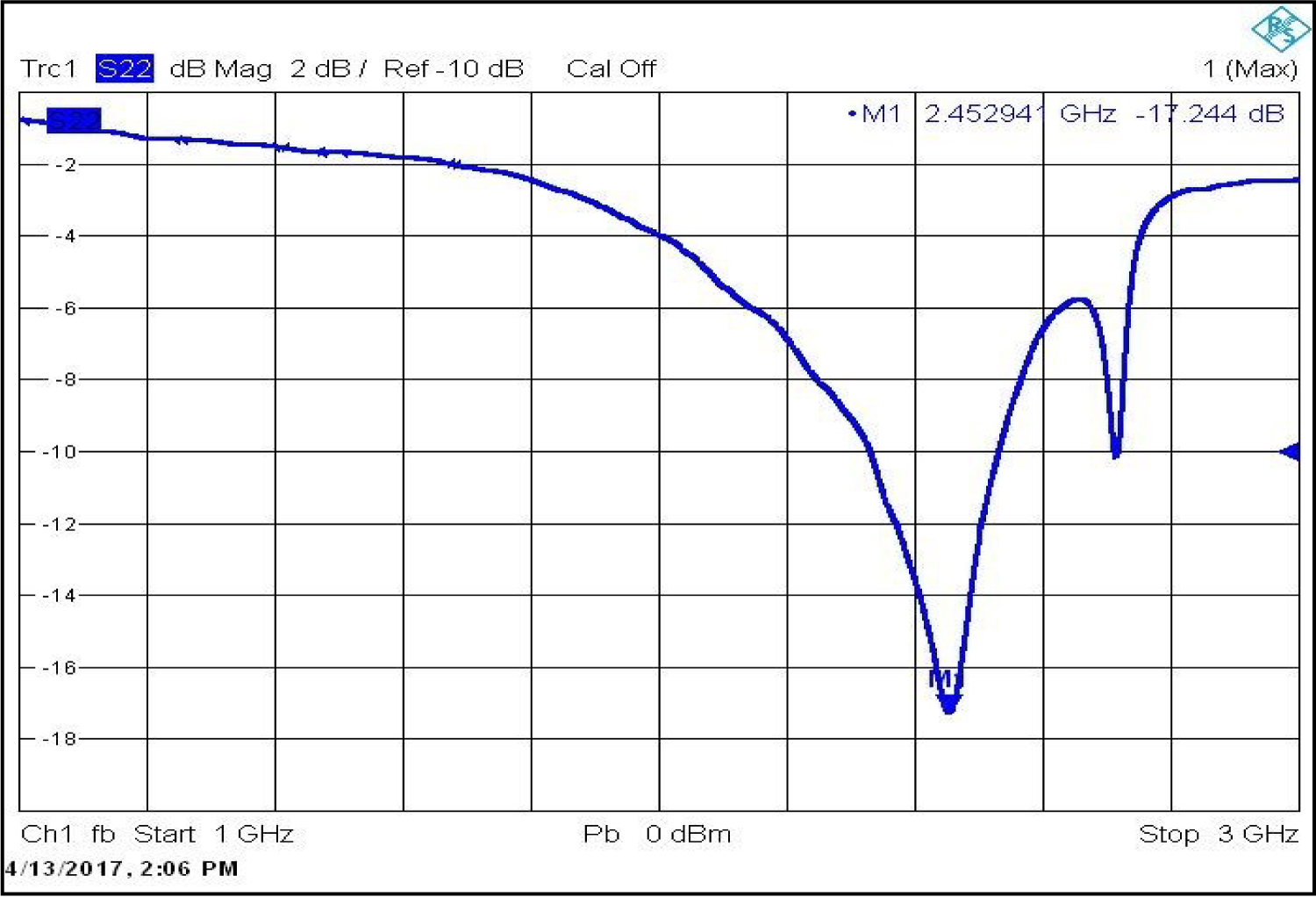
The antenna S11 concerning a 50 Ω impedance transmission line is illustrated. As seen, the value of the s-parameter from the spectrum analyzer is equal to s11 = -17.244 dB at 2.45 GHz. The s11 range is slightly shifted from the center frequency of 2.4 to 2.45 GHz as shown in Figure 12. This shift is probably caused by fabrication imperfections.
VSWR Parameter
As shown above, for the s11, the VSWR is measured for the fabricated Yagi antenna as shown in Figure 13. The value of the VSWR is equal to 1.336 at 2.4 GHz which is less than 2. This indicates that the fabricated design has a good matching and the fabricated design is successful.
Comparing between the Simulated and Measured Results
The comparisons between the simulated and measured results are presented in Figure 14 to Figure 15; In terms of the reflection coefficient (S11), Voltage Standing Wave Ratio (VSWR). In Figure 14, the reflection coefficient (s11-parameter) is plotted versus the frequency response around the center of the operating frequency (f0 = 2.4 GHz).
The measured reflection coefficient is found to be -17.244 dB, which is quite consistent with the simulated value of -28 dB. Simulated and measured results of the VSWR versus frequency are displayed in Figure 15. The measured and simulated results are in good agreement over the range from 2.3 GHz to 2.5 GHz. The measured value for VSWR is 1.336 at 2.45 GHz, while the simulation result shows a 1.3 value achieved at 2.4 GHz. Good agreements are also observed between the simulated and the measured results throughout the whole operating bandwidth. Both simulated and measured results provide highly acceptable matching between the antenna array and the feeding line at the operating frequency.
Conclusion
Seven-element microstrip Yagi antenna is proposed and fabricated with high directivity and gain for wireless communication. The finite integration technique (FIT) is employed for simulating the antenna array design. Different antenna parameters such as voltage standing wave ratio (VSWR), antenna gain, and efficiency have been studied. The antenna parameters have been tuned to achieve efficient matching and gain at the operating frequency (2.4 GHz). The obtained antenna gain of 12 dB is effectively reflected on performance enhancement in the desired frequency band.
In this paper, a proposed design of the microstrip Yagi-Uda antenna with a parabolic reflector is introduced and analyzed. The 3-D finite integration technique (FIT) is utilized to model the proposed design. It is found that the Yagi-Uda antenna showed ultra-high directivity of about 12 dB at a frequency of 2.4 GHz.
Moreover, the proposed design exhibits lower dissipation losses due to the S-parameter value is about -28 dB. Further, the Yagi-design is more compact with a small area, therefore it can be beneficial for the use in any microstrip-based MMIC circuitry.
In the experiment, a return loss of -17.224 dB is achieved at 2.45 GHz which indicates a good matching. Besides, the VSWR is equal to 1.336 at 2.45 GHz in good agreement with the simulated design. This design is applicable for wireless communications systems such as Wi-Fi, Bluetooth, and many other applications.
Further analysis will be carried out in the future to further enhance the VSWR value and to take into account the power radiated from the antenna design.


