
International Journal of Experimental Spectroscopic Techniques
(ISSN: 2631-505X)
Volume 5, Issue 1
Research Article
DOI: 10.35840/2631-505X/8524

Article Formats
Imaging Fourier Spectrometer in Visible Domain
Table of Content
Figures
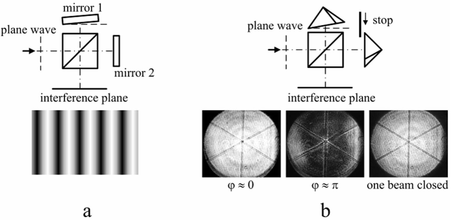
Figure 1: Interference of plane waves. In a standard....
Interference of plane waves. In a standard Michelson interferometer, tilting of any of the two mirrors produces a set of interference fringes (a). When mirrors a replaced by corner-cube reflectors, no fringes can be observed, although intensity of the image changes as the phase between the waves changes from 0 to (b).
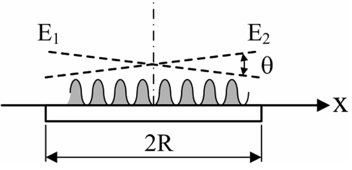
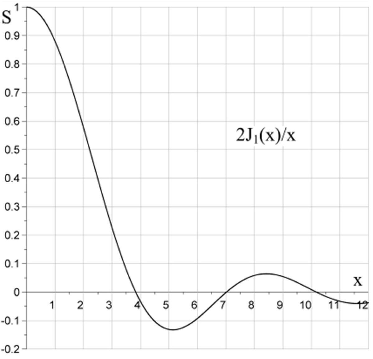
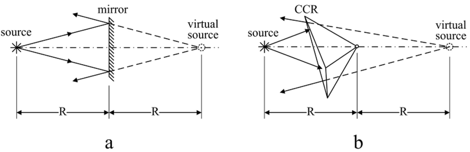
Figure 4: In a CCR, a cone of rays, after multiple....
In a CCR, a cone of rays, after multiple reflections, produce the virtual source exactly at the same position, as a flat mirror placed in the apex of the CCR.
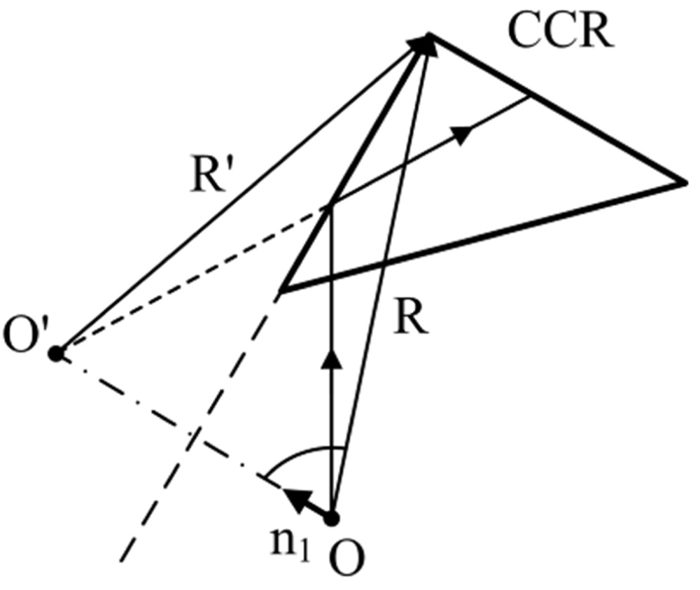
Figure 5: The source O at the origin is mirrored....
The source O at the origin is mirrored as a virtual source , when the ray reflects from the first face of the CCR.
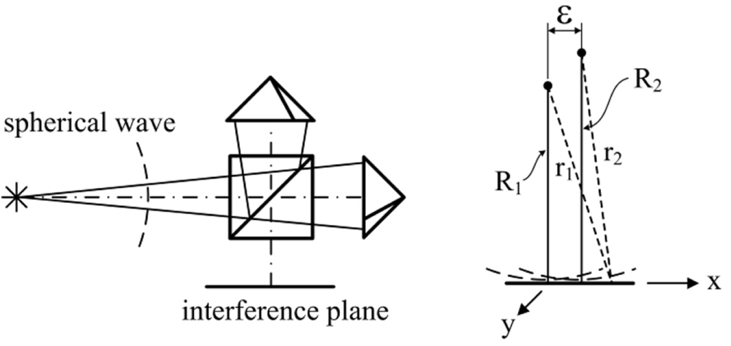
Figure 6: In the interference plane, the two CCR....
In the interference plane, the two CCR form two spherical waves, coming from virtual sources located at the distances and from the interference plane and laterally shifted by .

Figure 7: In the interference plane, the two CCR...
In the interference plane, the two CCR form two spherical waves, coming from virtual sources located at the distances and from the interference plane and laterally shifted by .
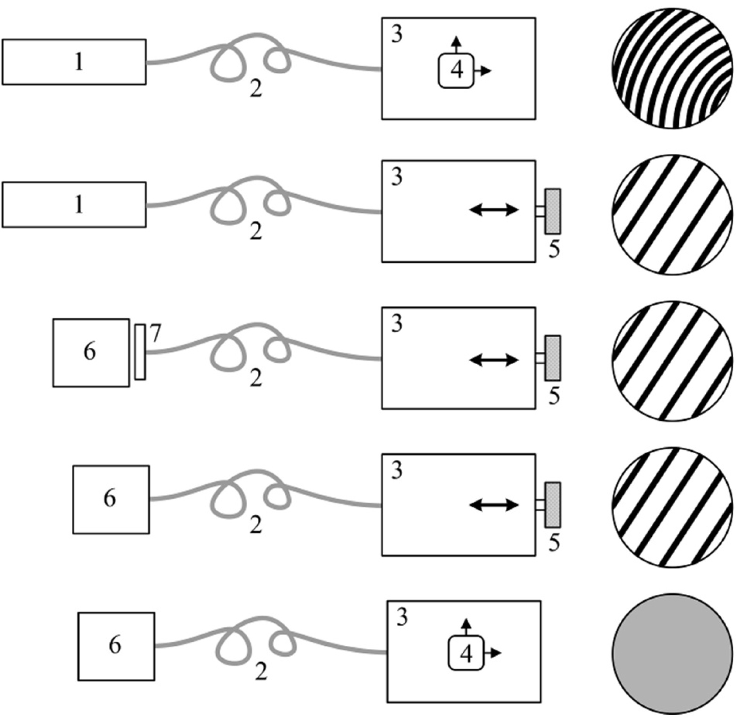
Figure 8: Alignment sequence. 1) He-Ne laser; 2) Optical...
Alignment sequence. 1) He-Ne laser; 2) Optical fiber; 3) Interferometer; 4) X-Y stage with CCR; 5) Translational alignment; 6) White light source; 7) Interference filter.
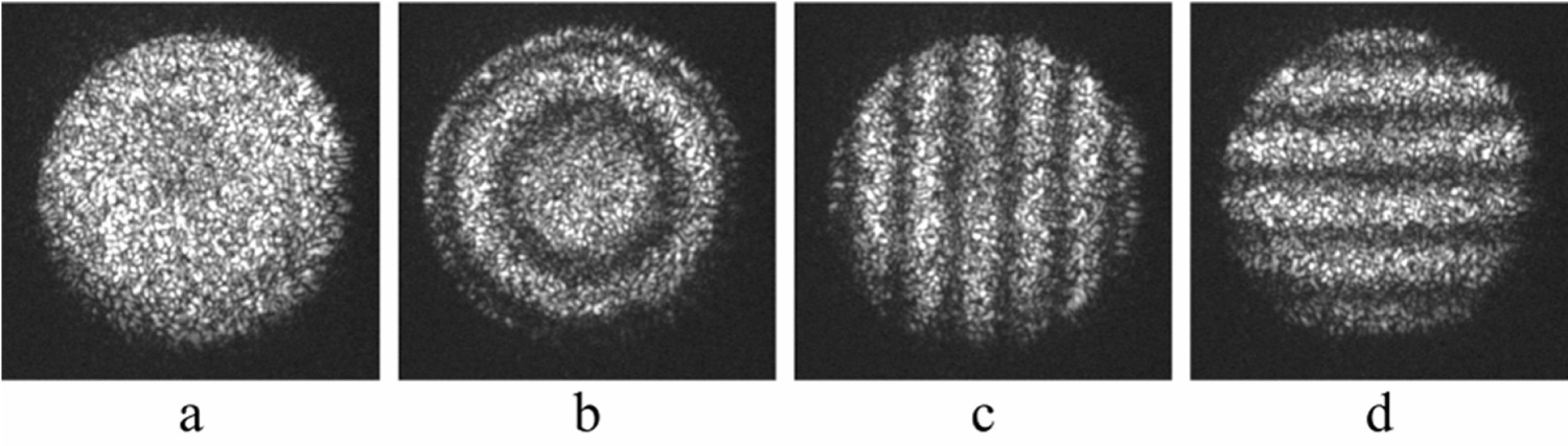
Figure 9: Possible interference patterns: a) Complete ...
Possible interference patterns: a) Complete alignment; b) Axial misalignment - inequality of optical paths; c) Horizontal misalignment; d) Vertical misalignment.
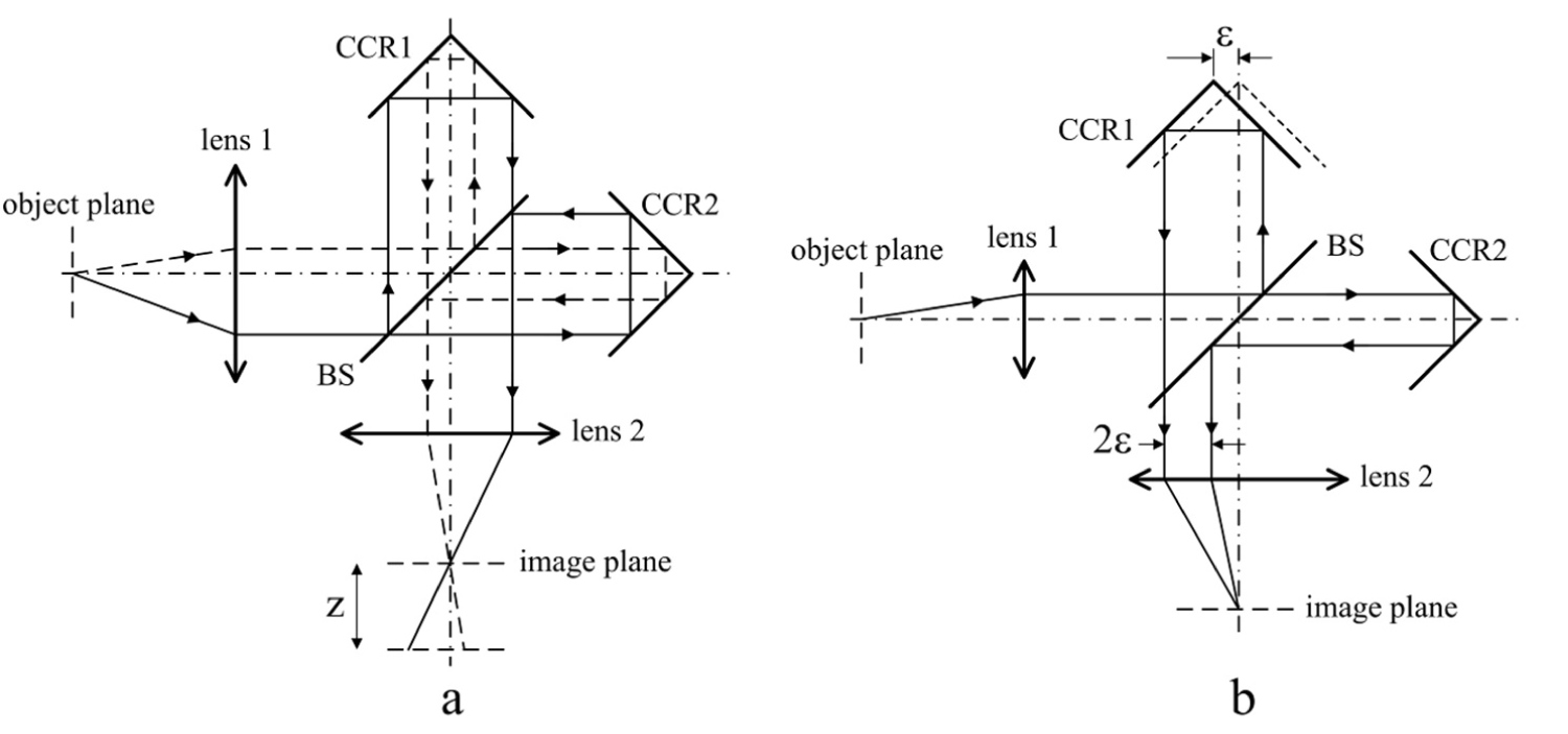
Figure 10: Generalized scheme of an imaging Michelson...
Generalized scheme of an imaging Michelson interferometer with CCR a) Perfectly aligned interferometer, when apexes of the CCR are mirror-reflected against the beamsplitter BS; b) Misaligned interferometer: Interfering rays are shifted by .
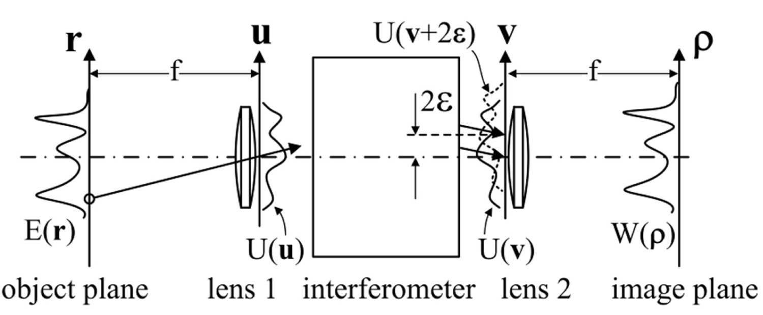
Figure 11: Equivalent optical scheme for the Michelson...
Equivalent optical scheme for the Michelson interferometer with CCR. Bold fonts denote vectors.
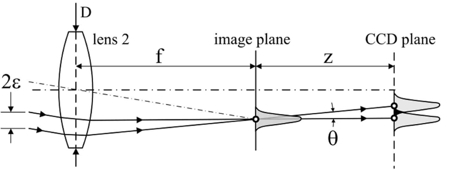
Figure 12: Interference takes place in the plane...
Interference takes place in the plane z only when point-spread functions of the two rays intersect.
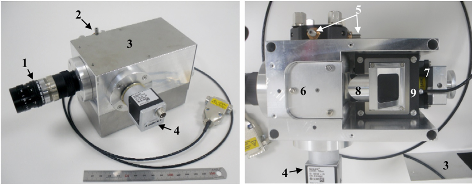
Figure 13: Opto-mechanical module of the reflectometer....
Opto-mechanical module of the reflectometer. 1- imaging optics (various types); 2- lateral adjustment stage; 3- cover plate; 4- high-speed CCD camera; 5- X-Y adjustment screws; 6- beamsplitter compartment; 7- manual positioner; 8- CCR; 9- piezo-scanner.
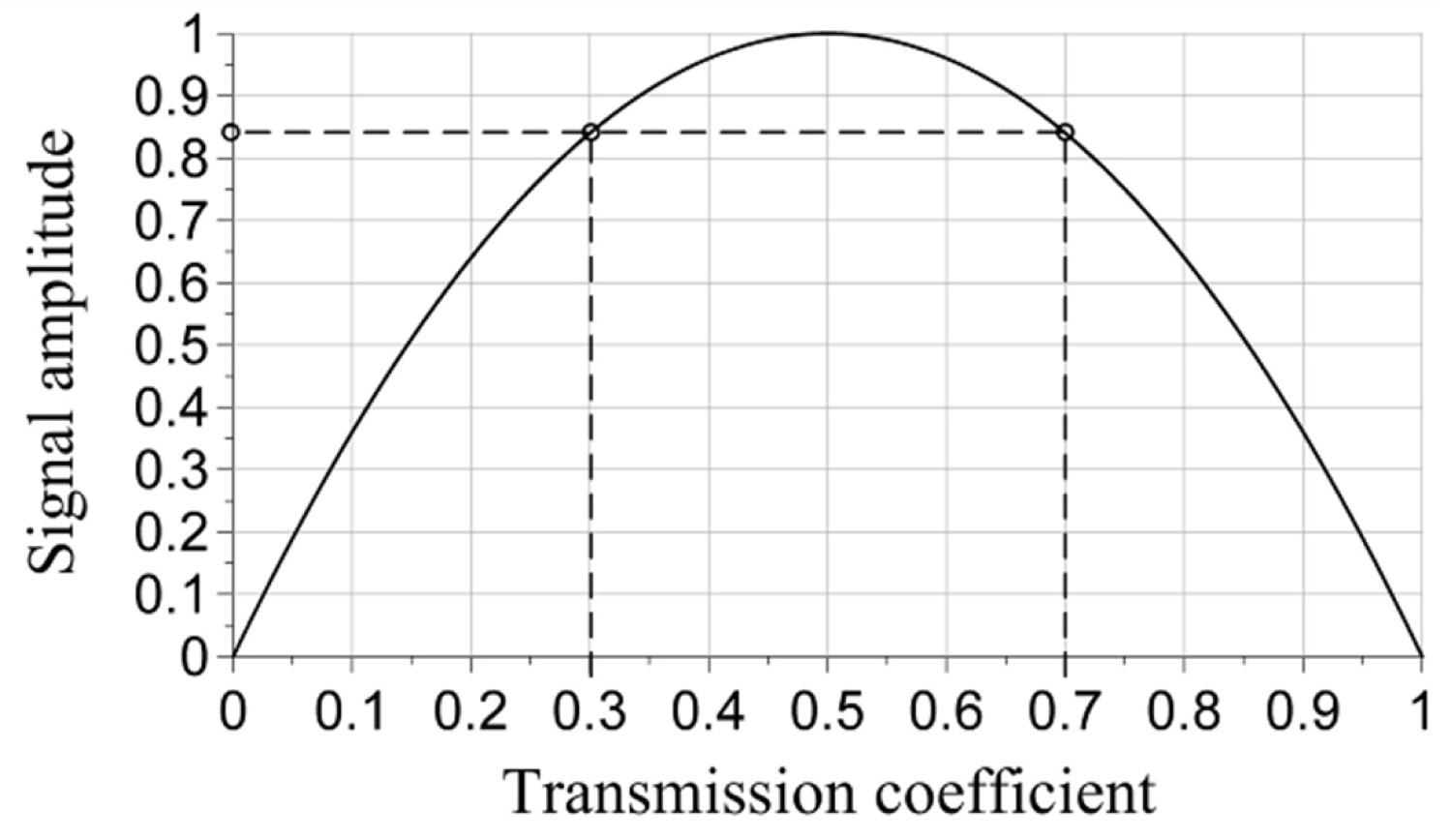
Figure 14: Normalized signal amplitude as a function...
Normalized signal amplitude as a function of the division coefficient.
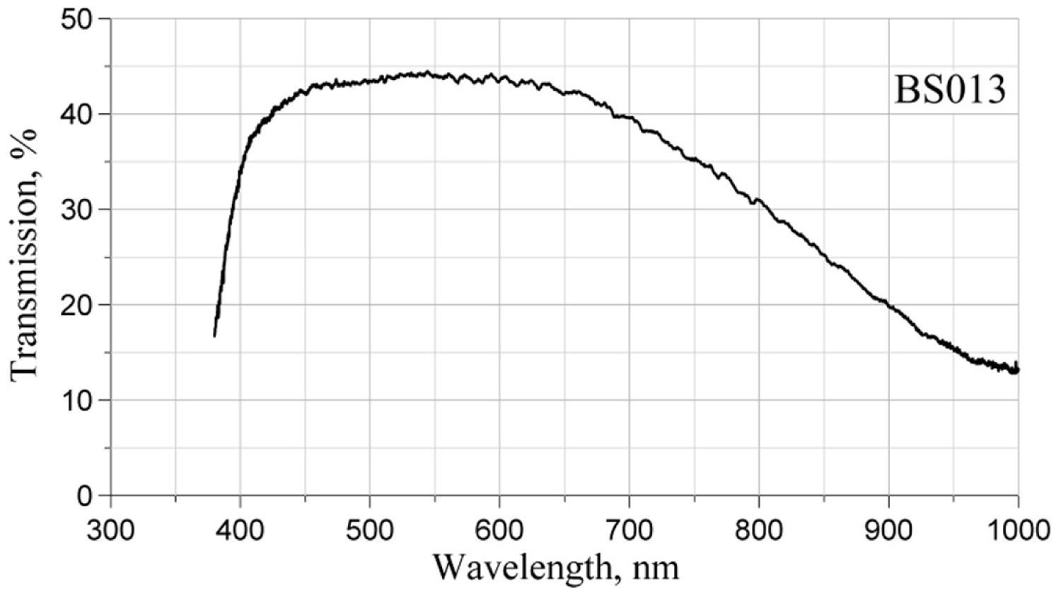
Figure 15: Spectral transmission of the BS013 beamsplitter....
Spectral transmission of the BS013 beamsplitter.
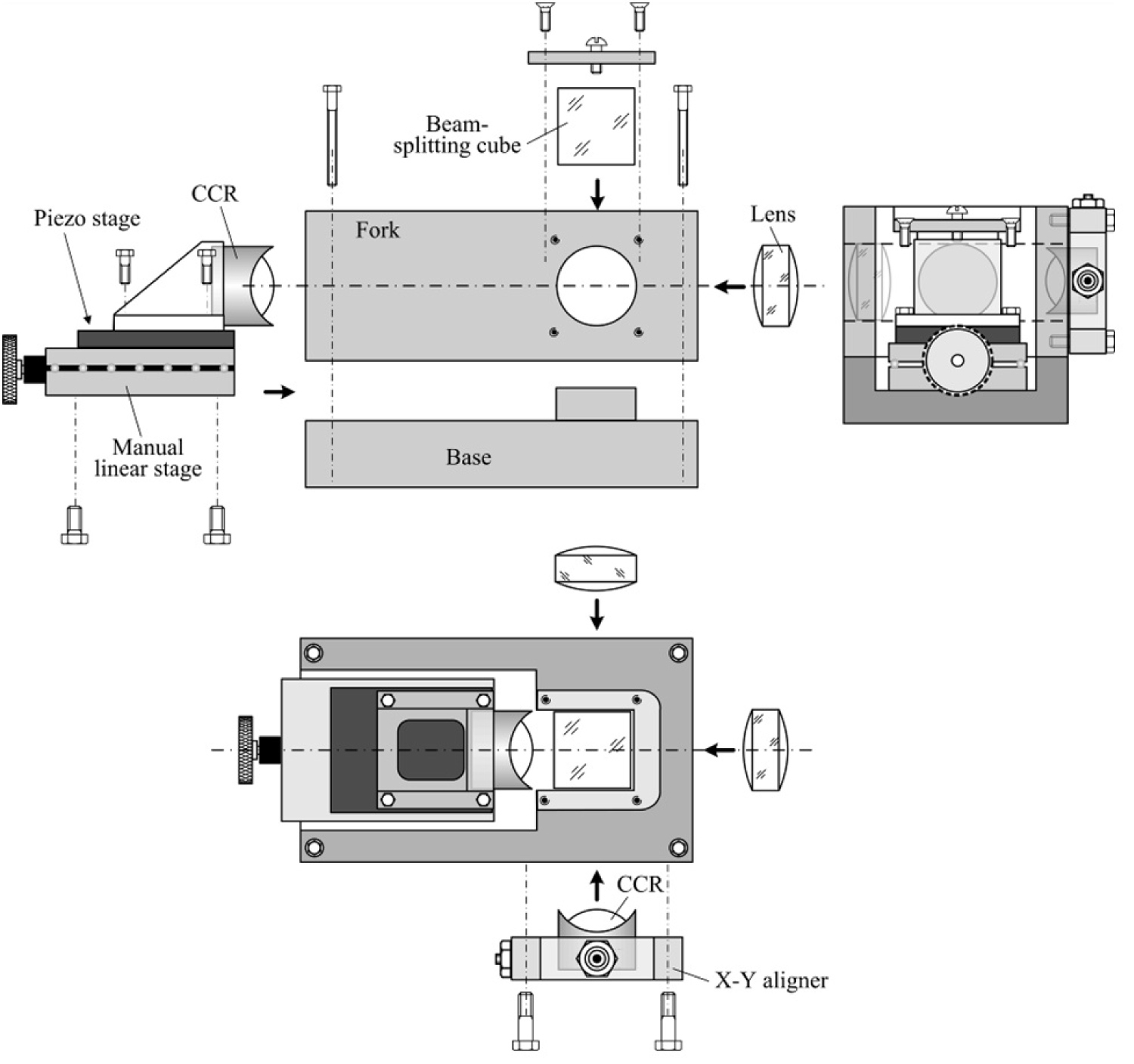
Figure 16: Three projections of the IFS design scheme....
Three projections of the IFS design scheme.

Figure 17: Typical spectra: white light source (top); Hg-Ar...
Typical spectra: white light source (top); Hg-Ar lamp (Ocean Optics HG-1; middle); ceiling LED lamp (bottom).
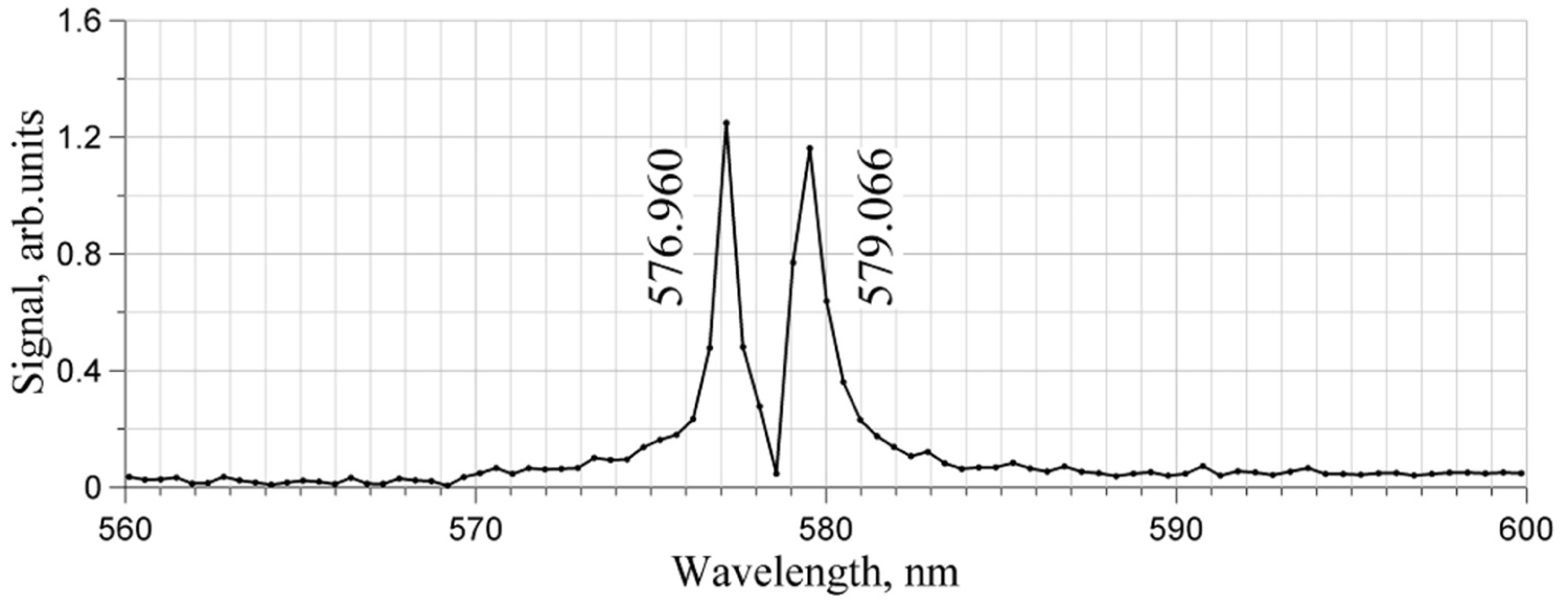
Figure 18: Close view of the mercury doublet around 570 nm...
Close view of the mercury doublet around 570 nm: The two lines separated by ≈2 nm are resolved.
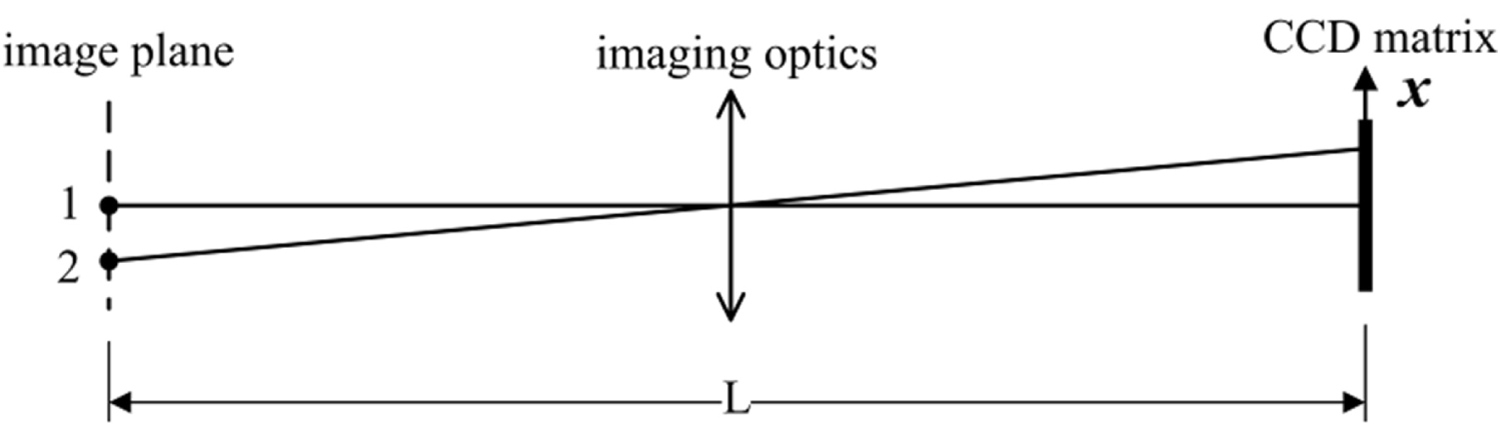
Figure 19: Generalized interpretation of optical paths...
Generalized interpretation of optical paths in imaging interferometer.
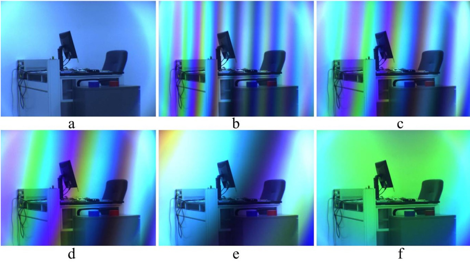
Figure 20: Pictures, obtained with the imaging reflectometer...
Pictures, obtained with the imaging reflectometer equipped with a 25 mm focal length front lens (Cosmicar/Pentax TV lens; part 1 in Figure 13). a) Fringe contrast is zeroed by setting big outside coherence range of light; b-e) ≈ 0, fringe contrast is a maximum, number of fringes decreases from 8 to 1 by aligning lateral position of the CCR; f) Nearly perfect alignment of CCRs - number of fringes < 1, fringe contrast is maximized ( ≈ 0).

Figure 21: Prototype of the imaging reflectometer: Opto-mechanical...
Prototype of the imaging reflectometer: Opto-mechanical parts (at left) and the control scheme (at right). 1) IFS; 2) Microscope unit; 3) Imaging optical fiber bundle; 4) White light fiber bundle; 5) CCD camera; 6) CCR; 7) Piezo-scanner; 8) Controller of the piezo-scanner; 9) DAC; 10) Computer.
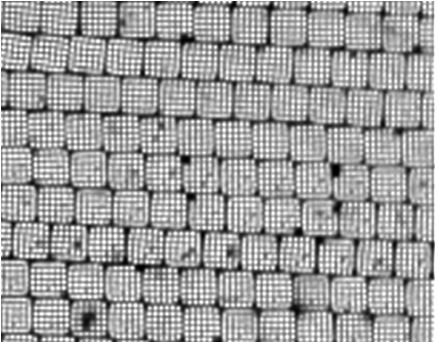
Figure 22: Microscopic structure of the imaging optical...
Microscopic structure of the imaging optical fiber bundle.
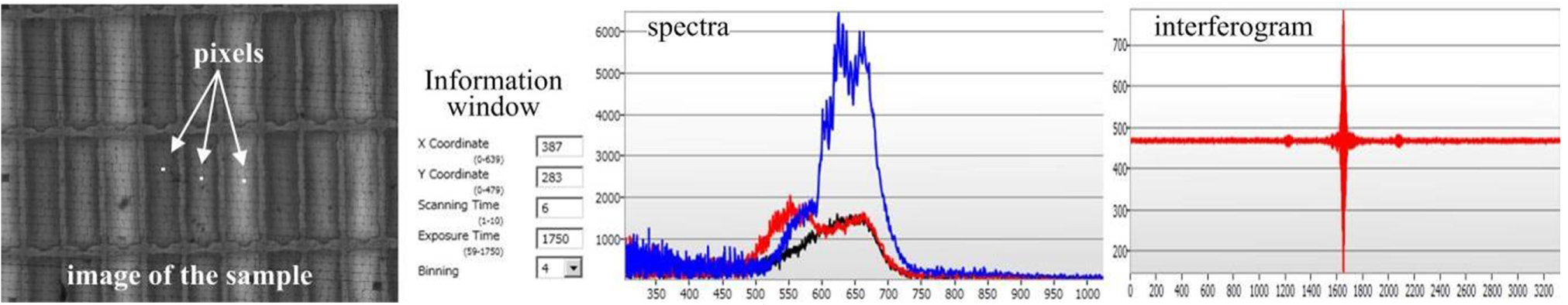
Figure 23: Principal components of the GUI (explained in the text)....
Principal components of the GUI (explained in the text).
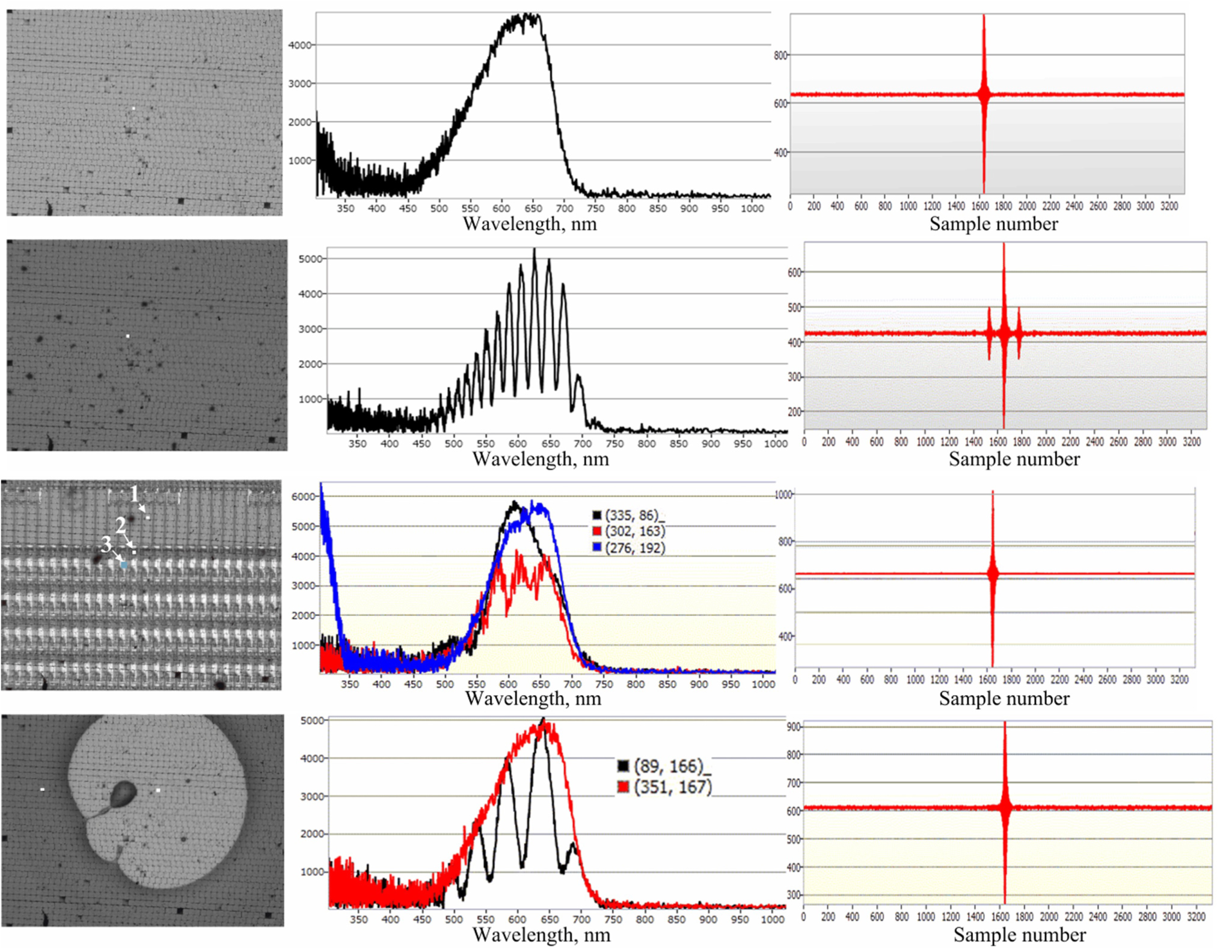
Figure 24: a) Bare silicon wafer; b) Silicon wafer coated...
a) Bare silicon wafer; b) Silicon wafer coated with 6 µ photoresist; c) Mobile phone LCD display (the interferogram relates to the pixel (335,86)); d) Spinner defect on silicon wafer (rounded light area is bare silicon, not coated with photoresist; the interferogram relates to the pixel (351,167)).
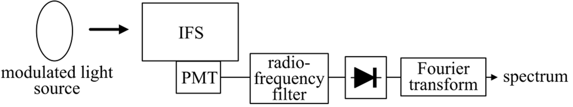
Figure 25: Principle of frequency-selective spectroscopy....
Principle of frequency-selective spectroscopy.
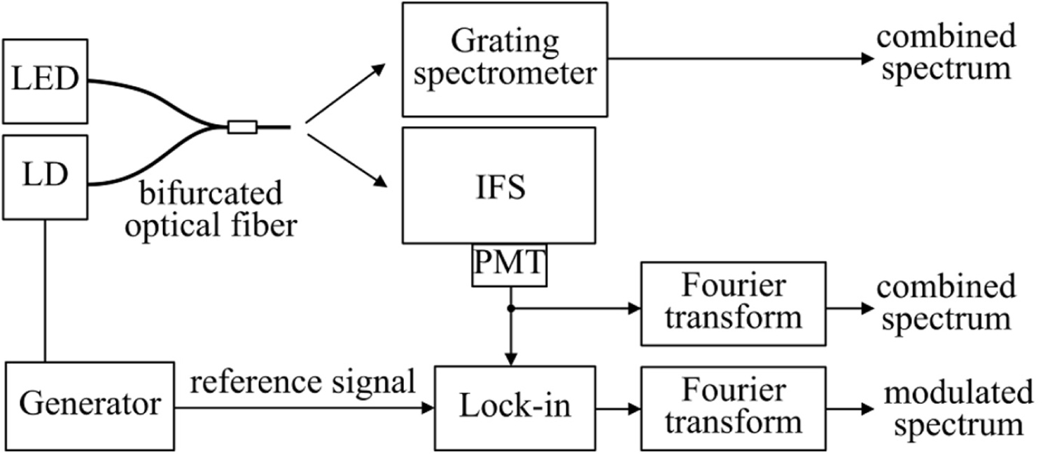
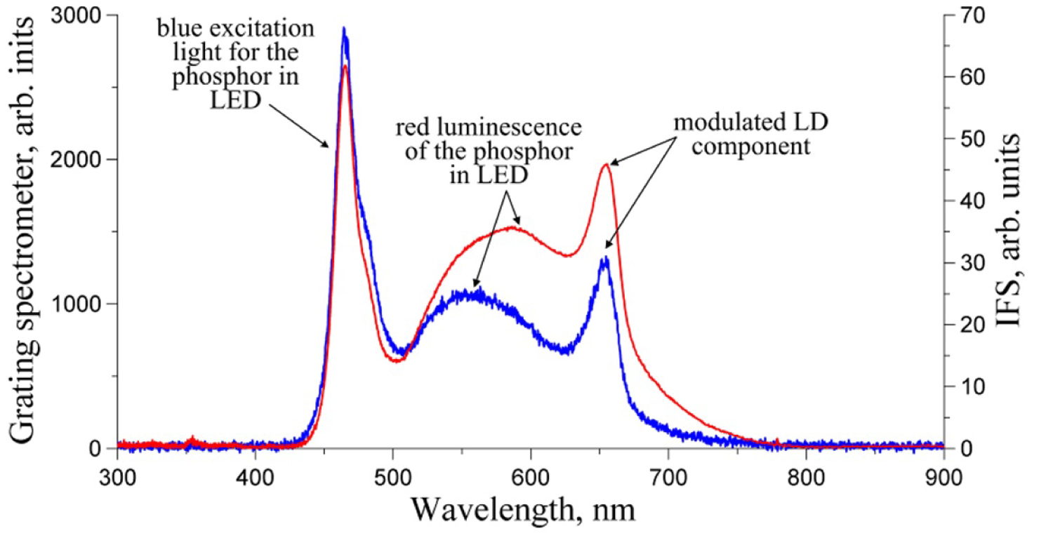
Figure 27: Combined spectra of the LED and LD measured...
Combined spectra of the LED and LD measured by the grating spectrometer (blue line) and IFS without filtering (red line).
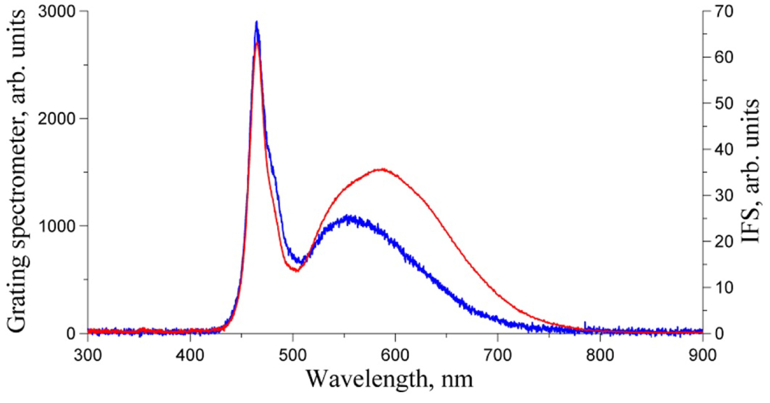
Figure 28: Only constant spectra from LED. Modulated signal is switched off....
Only constant spectra from LED. Modulated signal is switched off.

Figure 29: Comparison of the LD spectra in grating spectrometer and the IFS (non-filtered)....
Comparison of the LD spectra in grating spectrometer and the IFS (non-filtered).
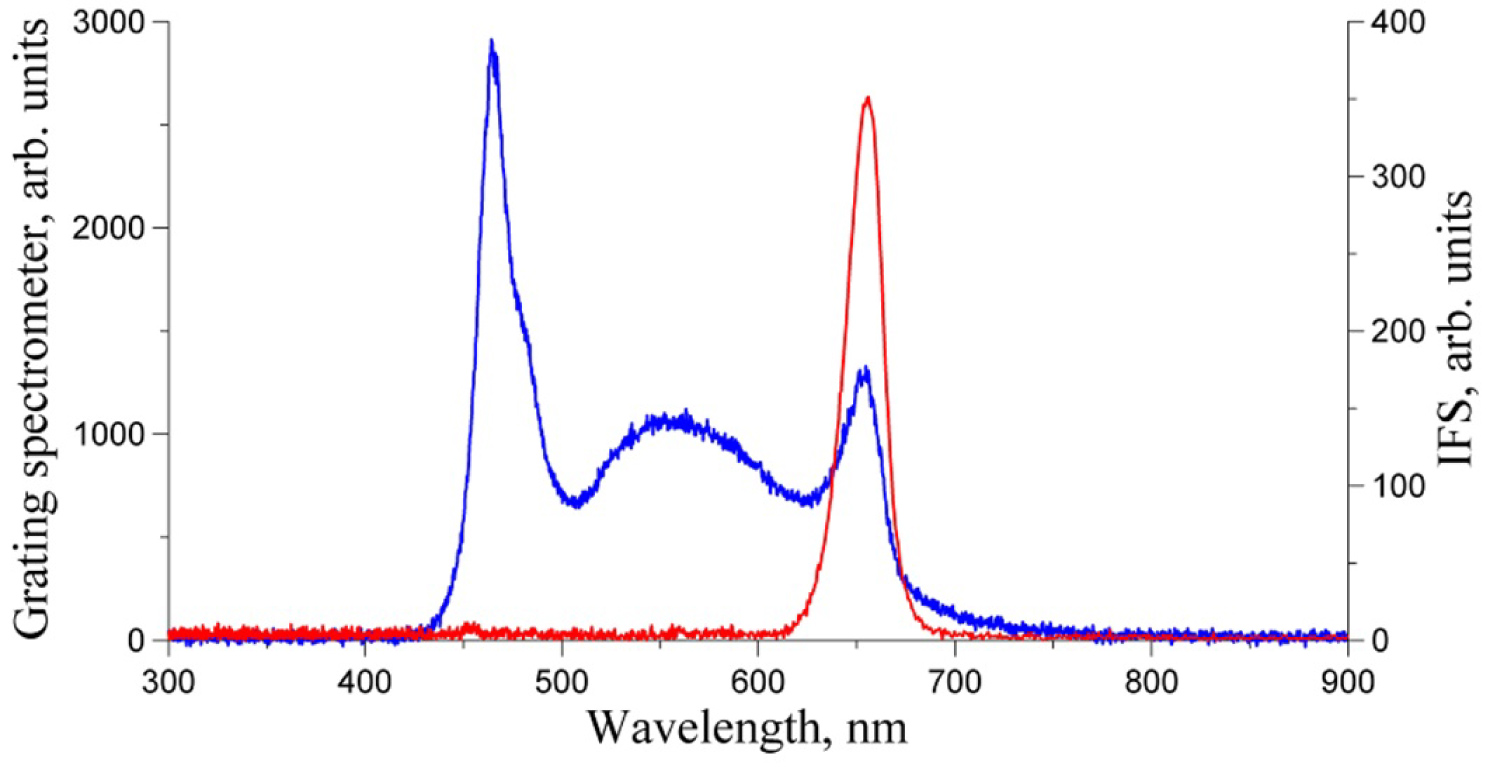
Figure 30: In comparison with the grating spectrometer...
In comparison with the grating spectrometer (blue line), modulated spectrum obtained from the IFS (red curve) shows complete removal of the non-modulated background.
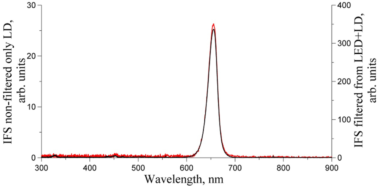
Figure 31: Comparison of the non-filtered (black line,...
Comparison of the non-filtered (black line, left axis) and filtered (red line, right axis) spectra of LD produced by the IFS.
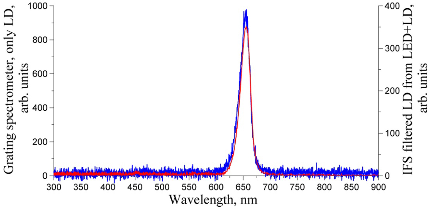
Figure 32: Comparison of the filtered IFS spectrum of...
Comparison of the filtered IFS spectrum of the modulated LD (red line) with the spectrum measured by the grating spectrometer (blue line).
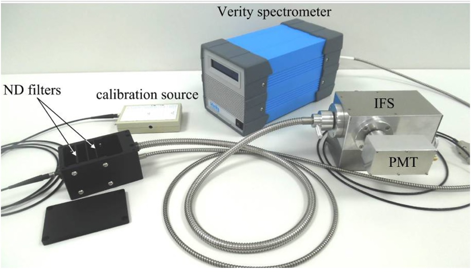
Figure 33: A set of neutral-density (ND) filters was...
A set of neutral-density (ND) filters was used to attenuate input optical flux from the calibration source.
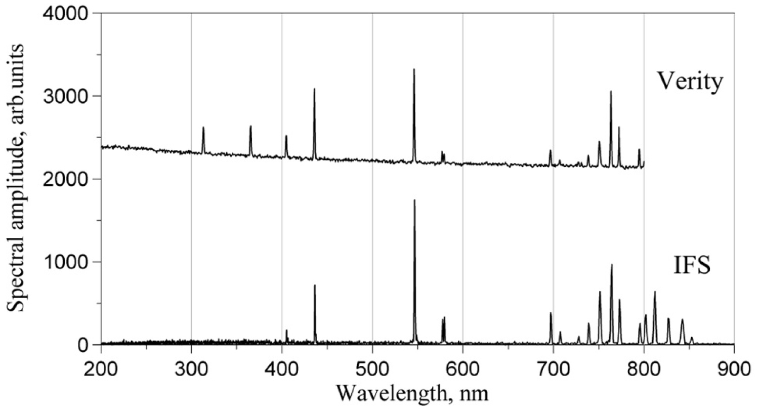
Figure 34: Comparison of spectra from Verity and IFS at ...
Comparison of spectra from Verity and IFS at medium optical flux.
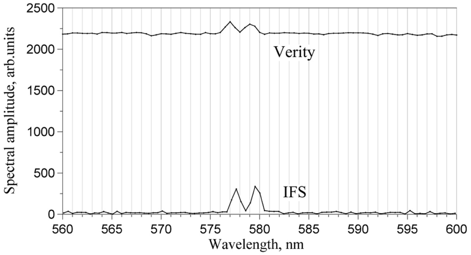
Figure 35: Magnified mercury doublet 576.960-579.066 nm....
Magnified mercury doublet 576.960-579.066 nm.
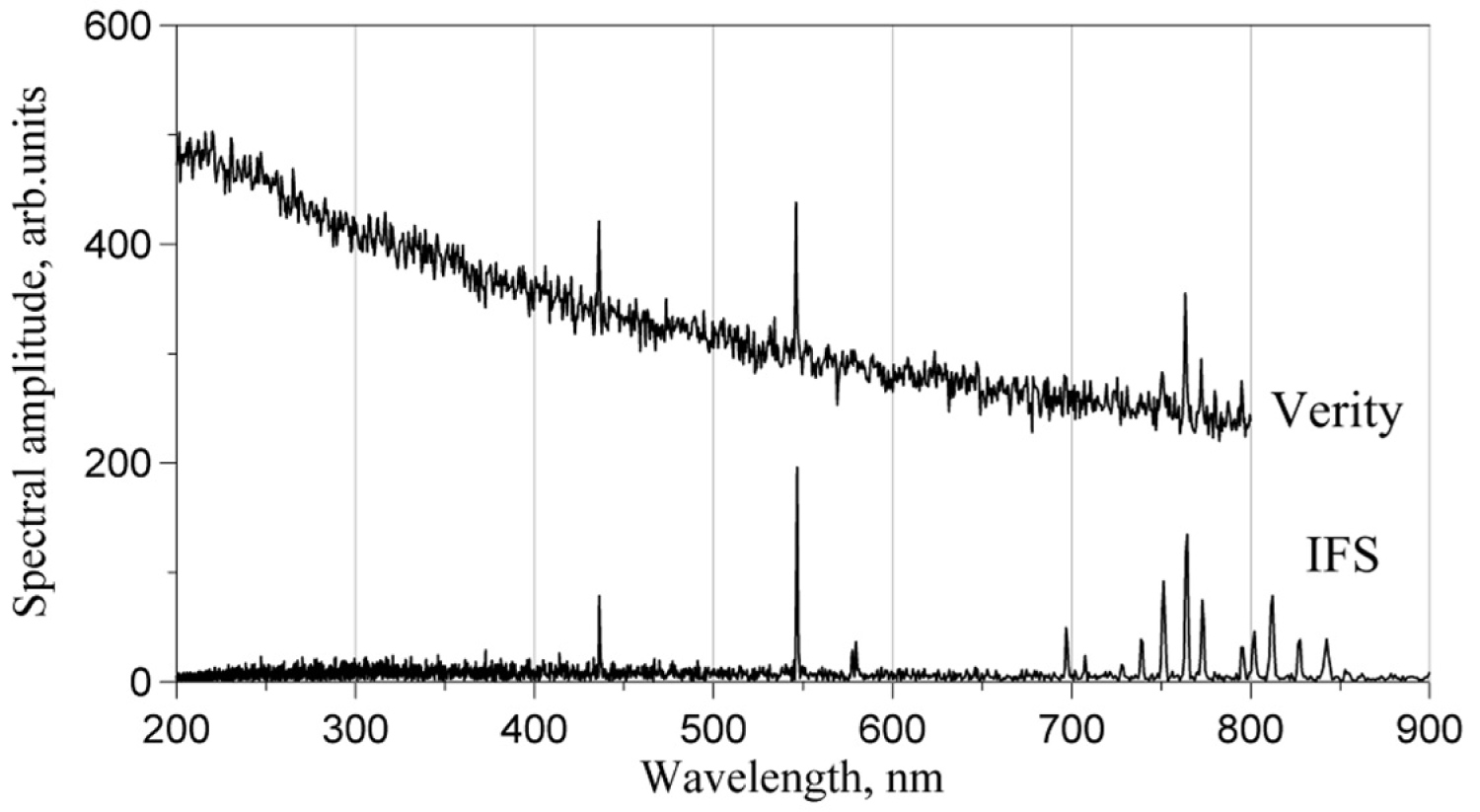
Figure 36: Comparison of spectra from Verity and IFS at low...
Comparison of spectra from Verity and IFS at low optical flux. The Hg doublet isn't seen in the Verity spectrum at all.
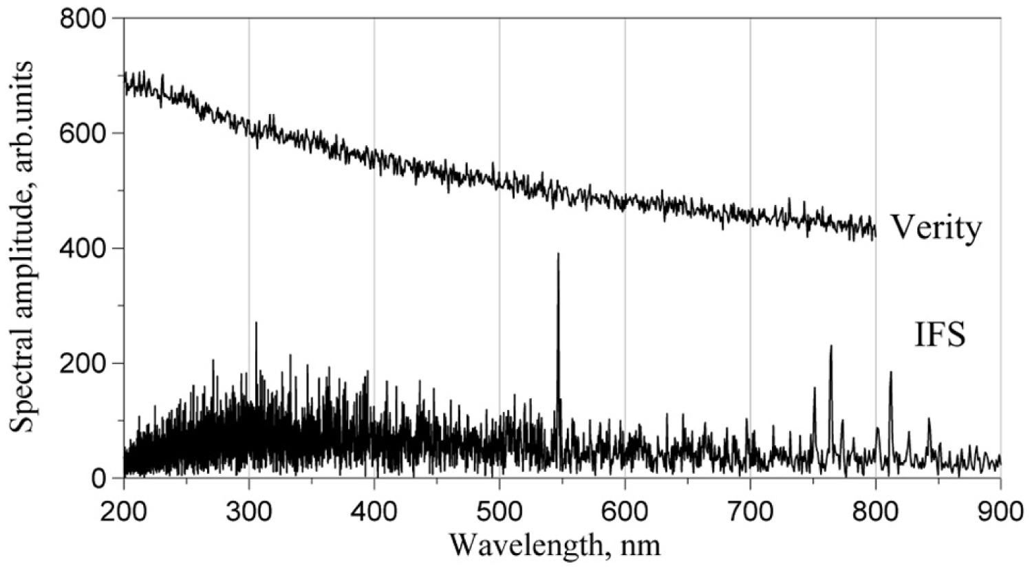
Figure 37: Comparison of spectra from Verity and IFS...
Comparison of spectra from Verity and IFS at ultra-low optical flux: 6.10-13 W/mm2.
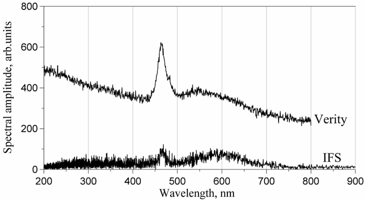
Figure 38: Combined spectra of the LED and LD measured...
Combined spectra of the LED and LD measured by the grating spectrometer (blue line) and IFS without filtering (red line).
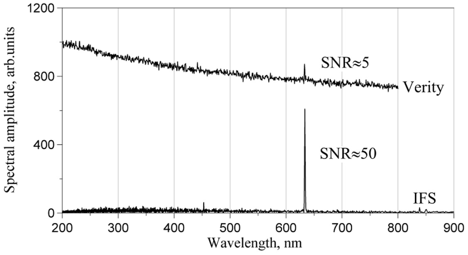
Figure 39: Combined spectra of the LED and LD measured...
Combined spectra of the LED and LD measured by the grating spectrometer (blue line) and IFS without filtering (red line).
Tables
Table 1: Characteristics of P-625.1 piezo stage.
Table 2: H6780-20 quantum efficiency.
Table 3: H6780-20 characteristics.
References
- E O'Neil (2004) Introduction to statistical optics. (4th edn), Dover Publications.
- JC Wyant (1978) Fringe localization. Appl Opt 17: 1853.
- VA Kotelnikov (2006) On the carrying capacity of the ether and wire in telecommunications. UFN 176: 762-770.
- http://ict.open.ac.uk/classics/1.pdf.
- P Nowakowsky, K Olexa, M Ray, P Fischione (2016) Precision top-down delayering of microelectronics. devices using broad-beam argon ion milling. The 16th European Microscopy Congress, Lyon, France.
- V Protopopov (2014) Practical opto-electronics. Springer, 393.
Author Details
V Protopopov*
Spectrella, Rakovo 57, Moscow District, Russia
Corresponding author
V Protopopov, Spectrella, Rakovo 57, Moscow district, 143523, Russia.
Accepted: February 13, 2020 | Published Online: February 15, 2020
Citation: Protopopov V (2020) Imaging Fourier Spectrometer in Visible Domain. Int J Exp Spectroscopic Tech 4:024
Copyright: © 2020 Protopopov. This is an open-access article distributed under the terms of the Creative Commons Attribution License, which permits unrestricted use, distribution, and reproduction in any medium, provided the original author and source are credited.
Abstract
A prototype of an imaging Fourier spectrometer, with corner-cube reflectors in the Michelson interferometer, is developed for visible and near-infrared domains. The use of corner-cube reflectors enables stability of operation, while imaging capability makes wide field of view and, consequently, increases input optical signal. In imaging mode of operation, optical signal is recorded by high-speed camera, enabling spectral measurements in each pixel of the image. Imaging spectral reflectometry is experimentally demonstrated. In high-frequency applications, optical signal is recorded by a photo-multiplying tube. Selectivity of spectra modulated at 100 kHz on the background of non-modulated light is experimentally demonstrated. On line-type spectra, with the same exposure time and spectral resolution, the imaging Fourier spectrometer may be 10 times more sensitive than the best compact grating spectrometers. This superiority disappears on wide spectra. In visible and near-infrared domains, a carefully made prototype of an imaging Fourier spectrometer with a photo-multiplying tube proved to be sensitive to as low optical flux as 6.10-13 W/mm2.
Index Headings
Michelson interferometer, Corner cube reflector, Fourier spectroscopy, Imaging spectroscopy, Modulation-sensitive spectroscopy, Spectral interferometry, Spectroscopic sensitivity, Interference, Interferogram, Spatially resolved spectroscopy
Introduction
After centuries of progress in spectroscopy, it seems that there cannot be any meaningful spectroscopic task that is not supported by instruments available on the market. However, science and technology go ahead, and new applications do emerge that suggest very special requirements to spectrometers. At least three of such applications are clearly identified by the progress in semiconductor industry and biology:
1. Imaging spectrometers in visible and near-infrared domains - tools that measure spectra in every pixel of the magnified image of a sample;
2. Frequency-selecting spectrometers that measure only modulated component of the optical flux, selecting it from non-modulated background;
3. Super-sensitive spectrometers in visible domain that can overcome theoretical limit of traditional grating spectrometers.
The first of these was brought into spotlight by achievements in semiconductor manufacturing and biology. In semiconductor industry, quality of nano-scale patterns is commonly estimated by spectral interferometry. Traditionally, spatial resolution of spectral interferometry is determined by the size of a focused white-light beam that illuminates the pattern. This focal point is a projection of an optical fiber, delivering light from the source, and therefore, cannot be made as small as the optical resolution of a microscope used for the measurement. With the scale of semiconductor patterns quickly going down below micrometer range, the limitation of traditional spectral interferometers became an obstacle. In biology, fluorescence spectra of living cells must be measured in each pixel of highly magnified image without time-consuming two-dimensional scanning - the task that cannot be solved, using traditional spectrometers.
The second task belongs in semiconductor manufacturing, biology, and, to some minor extent, in inspection of overhead power lines and military domains. Nano-scale structure of semiconductor devices is created in etching machines - plasma chambers, filled with active gases that efficiently remove (etch) nano-patterned areas on silicon wafers. The plasma is sustained by applying high-frequency voltage to the electrodes inside the chamber, leading to modulation of optical emission at frequencies about hundreds of kilohertz. Since spectrum of optical emission is nowadays almost the only way to monitor status of the etching process, it is important to select modulated component on the background of non-modulated spectrum. In biology, metabolism of leaving cells may be studied by measuring fluorescence of macro-molecules under excitation of modulated violet or ultra-violet light. This fluorescence, also modulated and shifted in phase relative to the excitation pulse, is usually weak and has to be detected on strong background of ambient light. Probably less important, but still existing application is to measure spectra of high-voltage coronas around electrical power-transmission lines: This light is 60 or 50 Hz modulated, which opens a possibility of its efficient detection not only at night but also during daylight.
As to the third requirement stated above, sensitive spectrometers were always in demand regardless particular application. There are limitations to sensitivity of every grating spectrometer, determined by fundamental reasons - physical and technical: Input optical aperture and quantum efficiency of the photodetector. For a grating spectrometer, input optical aperture is always a slit, whose dimensions are limited: Width - by required spectral resolution, and height - by vertical dimension of the photodetector matrix. For the spectrometers on the market, typical slit width is around 20 microns, determining standard spectral resolution of about 1.5 nm - acceptable for the most applications of such devices. The height is limited by vertical size of a multi-element photodetector array (typically charge coupled devices - CCD), which never exceeds 8 mm because the optical scheme of the spectrometer cannot relay longer images from the slit plane to the detector through diffraction grating without loss of image quality. Thus, maximum practical input aperture of the grating spectrometer cannot exceed 0.02 × 8 ≈ 0.16 mm2. For the most advanced CCD matrices, available today - back-thinned, thermo-electrically cooled - quantum efficiency in a single sensitive element (pixel) is more than 0.9, and cannot be bigger than 1.0. Thus, here is the limit of sensitivity of grating spectrometers that cannot be overcome, and various models differ from one another by numerical factors about 2, depending on transmission efficiency of particular optical schemes, relaying input optical flux through the grating to the photodetector. What else can we think of, if we need even higher sensitivity?
The present publication describes a prototype of a spectrometer that may be a solution to all three applications above: Imaging Fourier Spectrometer (IFS) with corner-cube reflectors (CCR) in visible and near-infrared domains. The material below is logically divided into five main parts: Theory of IFS with CCR; opto-mechanical design and data acquisition; imaging capabilities; selection of modulated spectra; and comparison of the IFS sensitivity with the state-of-the-art grating spectrometer.
Theory of the Michelson Interferometer with Corner-Cube Reflectors (CCR)
Basic considerations for the interferometer
The Fourier spectrometer is based on the Michelson interferometer, which is traditionally understood as a combination of two plane mirrors and a beamsplitter between them (Figure 1a). Assume for the beginning that perfectly plane wave comes to the interferometer. If mirror 1 is tilted relatively to mirror 2, then interference fringes are observed in the image plane.
In the Fourier spectroscopy, modulation of light in the image plane is measured by a photodetector and then processed mathematically to reconstruct the spectrum of light. Therefore, amplitude of the electrical signal is important. In order to maximize this signal, the number of fringes within the sensitive area of the photodetector should be as small as possible. Indeed, consider a photodetector with circular sensitive area of radius R, at which two plane waves come with the angle between them (Figure 2).
One of the waves has variable phase , accounting for the displacement of one of the mirrors in the interferometer. The interference pattern is then the oscillating intensity with constant pedestal:
With being the wave number. Only the second oscillating term in the right-hand side of (1) contributes to the useful electrical signal of the photodetector, and we are interested in its amplitude A. Integration over the circular area with polar coordiniates r and α gives the electrical signal:
Where the term with vanishes as the integral of the odd function over symmetrical area. Thus, the amplitude of modulation is
Where is the Bessel function of the first order. The number of fringes N over the photodetector can be easily expressed through the phase increment over the diameter:
Leading to a simple formula:
This function, known as the Airy function, is shown in Figure 3.
Negative values indicate the change of phase in the output electrical signal. If the signal must not fall below 0.8 of its maximum, then the number of fringes must be less than 0.4. With one fringe on the diameter, the amplitude of the signal falls to 0.2 of the maximum. Therefore, a very accurate angular alignment of mirrors must be done, with accuracy of about angular minutes, which is a big disadvantage of the mirror-type Michelson interferometer. Moreover, in visible domain, which is our priority for the reasons explained in the introduction section and where the wavelength is short, alignment tolerances of this type of the interferometer become so severe that make the mirror-type interferometer impractical. To overcome this drawback, corner-cube reflectors (CCR) may be used. A CCR reflects incoming plane wave back in exactly the same direction, regardless any tilts relative to the direction of the coming wave. Therefore, all spatial parts of interfering plane waves are equally dephased, producing no interference fringes and, hence, maximizing the signal of the photodetector (Figure 1b). Thus, CCR greatly improve stability of the Michelson interferometer, at least for perfectly plane waves.
Basic properties of CCR
Plane waves do not carry information about the image: A plane wave produces a point-like spot in the focal plane of a lens - not the image. Therefore, if we want to relay an image through the interferometer, we have to consider a conical wave and to understand the requirements that conical waves impose on the alignment procedure of the interferometer. For that, it is sufficient to analyze a simplified model: A cone beam produced by a point source (Figure 4). It will be shown that a CCR acts exactly as a flat mirror, producing a virtual source on the axis, connecting its apex and the source, at the distance equal to the distance between the source and the apex. Regardless orientation of the CCR.
Let the source be positioned in the origin O and the apex at the point determined by the vector R (Figure 5). Reflection from the first face of the CCR creates a virtual source . The unity normal vector to this face is . Taking the first virtual source as the origin, the apex of the CCR is positioned at the point defined by vector :
Where round brackets denote a scalar product. From here
The second face of the CCR is defined by the unity normal vector , and reflection from the second face creates the second virtual source , which is connected to the apex by the vector :
The third and the final reflection from the face defined by the unity normal vector creates virtual source with the vector , connecting it with the apex:
Then position of the final virtual source, relative to the physical source located at O, is defined by the vector . Computing from (6)-(8), using orthogonality of the normal vectors for , we obtain:
Vectors n1, n2, n3 form the Cartesian system of coordinates with the origin at the apex of the CCR, in which the scalar products are none others but directional cosines of the vector R. Therefore,
And
Which means that, after triple reflection from the CCR, the virtual source is positioned on the axis, connecting the physical source and the apex, at the distance from the physical source, as shown in Figure 4b. This result holds true for any tilts of the CCR relative to the source: only position of the apex is important.
In the section 2.1, interference of plane waves in the Michelson interferometer was outlined and it was emphasized that, for the plane waves only, the interferometer with CCR does not produce any fringes. Now, consider what happens when conical beams interfere in the Michelson interferometer with CCR (Figure 6).
Interference pattern in the plane is defined by the intensity of the sum of two spherical waves with the wavelength , coming from virtual sources located at the distances from the point of observation:
Where . Considering, as usual, long , and using the first-order expansion of , obtain:
The origin of the system of coordinates in the interference plane was chosen in the projection of the first virtual source. The phase determines interference pattern: Quadratic terms in produce curvature of fringes, while linear term in is responsible for the straight fringes. When , i.e. optical paths to the CCR are equal, quadratic term vanishes. When apexes of the CCR are located on one line, i.e. = 0, linear term vanishes. A set of three typical simulated pictures is shown in Figure 7. It gives us a very important hint on the alignment procedure for the Michelson interferometer with CCR: (A) If the interference fringes display curvature, then equalize optical paths in the shoulders of the interferometer until straight lines appear; (B) After that, align lateral displacement of the one of the CCR until uniform illumination replaces fringes. Thus, unlike the case of the interferometer with mirrors, requiring angular alignment of the mirrors, alignment of the interferometer with CCR requires lateral displacements of the CCR. This feature makes the Michelson interferometer with CCR far more stable relative to its mirror-based analog.
The alignment sequence is outlined in Figure 8. It starts with connecting the interferometer to a He-Ne laser in order to obtain initial picture with interference fringes, shown schematically at right. Coherence length of the He-Ne laser radiation is on the scale of kilometers, making the two waves interfere at any initial path difference that occurs in the interferometer without preliminary equalization of optical paths. An important feature of the interferometer with CCR is that the curvature of fringes indicates the optical path difference between the two shoulders: The more the curvature, the bigger is the path difference. Therefore, at the next step, the second CCR installed on a piezo-scanner is manually moved to and fro so that to minimize the curvature of fringes. Although this operation does not guarantee complete equality of optical paths in the shoulders, it minimizes the optical path difference to a value when interference fringes can be visible with interference filter and white light source. Next, the laser is substituted with the white light source (tungsten halogen lamp) and interference filter at its output. Coherence length shortens to a scale of hundreds of microns, and it is not very difficult to maximize interference contrast to further minimize the optical path difference between the shoulders. Only axial positioner is activated at this phase, leaving interference fringes visible as a mark for estimating the contrast. After that, interference filter is removed and fine axial alignment is done, maximizing fringe contrast again. Finally, the X-Y positioner of the first CCR is used to completely remove fringes from the image.
As additional explanation, Figure 9 portrays the images obtained with laser illumination in four different cases of alignment. Note, that the image with concentric circles cannot be achieved in white light illumination because in this case the optical path difference greatly exceeds coherence length of light.
Imaging configuration of the Michelson interferometer with CCR
Generalized optical scheme of the imaging Michelson interferometer with CCR is shown in Figure 10. According to the Fermat principle, all the rays, emerging from any point in the object plane and converging to its image point (conjugated point) in the image plane, have the same traveling time through their paths. It means that all the conjugated points in the object and image planes are temporally coherent, i.e. have the same phases. Therefore, the waves, forming images of these points, interfere in the image plane. It does not matter, whether the object plane coincides with the focal plane of the lens 1 or not: Temporal coherence between all the rays from a single point in the object plane will be preserved in the conjugated point in the image plane. As such, the electrical signal from every pixel of an image sensor, placed in the image plane, will be accordingly modulated when one of the reflectors is being moved along the axis, exactly as in a non-imaging Fourier spectrometer. Thus, making standard mathematical computations on the signals from every pixel of the image sensor, it is possible to reconstruct spectrum of light in every pixel. This is the idea of an imaging Fourier spectroscopy.
In a perfectly aligned interferometer, the two rays, in which the beamsplitter splits any single ray coming from the object, recombine in a single ray again. In Figure 10a, the two arbitrary chosen object rays are shown in solid and dashed lines, splitting at 90° at the beamsplitter and recombining again before they are directed to the lens 2. Since the rays coincide, they propagate with constant phase difference and interfere at any point on their trace. It means that in a perfectly aligned interferometer, interference pattern is not localized in the image plane only and may be observed at any displacement z from it. The image is distorted outside the image plane, but interference pattern is observable.
Consider now what happens when one of the CCR is shifted by a distance : The rays, being split by the beamsplitter, do not recombine again and are shifted by (Figure 10b). The equivalent optical scheme in Figure 11 is helpful to address this problem mathematically. For the sake of compactness of formulas, we may assume equal focal lengths f of the lenses 1 and 2. If they are not equal, then a trivial scale coefficient will appear in the final result. Let be spatially incoherent complex field with the wavelength in the object plane, and its intensity being . Then the field at the output pupil of the lens 1 is proportional to the Fourier transform of [1]:
With integration over the entire plane r, and being the wave number. The interferometer with CCR creates the second wave and directs both the original and the new waves in the mirrored direction to the second lens. Dropping the proportionality coefficient and assuming 50% splitting of the original wave, the two interfering waves at the input pupil of the lens 2 are and . In the image plane , the first and second interfering waves create complex fields and , so that the average intensity is
Where the asterisk denotes complex conjugate. Since any waves at the input pupil of a lens and in its image plane are Fourier-inversed according to (15), it is possible to write down:
These formulas are approximate to the extent to which the integral over the lens pupil may be assumed the delta-function:
Which means high spatial resolution of the lenses.
With (17) and (18), formula (16) gives the intensity in the image plane:
The factor «2» vanishes because the beamsplitter relays only half of the original intensity in each shoulder of the interferometer: . Thus, the image plane of the misaligned Michelson interferometer with CCR reproduces the intensity in its object plane with fringes . Note, that the mirror-based Michelson interferometer would give the inverse intensity distribution, proportional to .
Next we are going to discuss localization of fringes - the feature of the interferometer that determines how accurately the photodetector may be positioned in axial direction relative to the output image plane. According to the principle formulated in reference [2], «the fringe viewing surface for an interferometer should be the surface that is the locus of points of intersection of the rays which originate from one incident ray coming from the source». Figure 10b indicates that, in our case, such locus is the output image plane, where the contrast of fringes is a maximum regardless relative displacement of CCRs . It means, that placing the photodetector exactly in the output image plane, the maximum sensitivity of the spectrometer is guaranteed. But how accurately it must be positioned and how big the fall of sensitivity will be if actual position of the photodetector is shifted by value z from the image plane (Figure 10a)? Geometrical optics cannot answer this question, therefore, we have to consider diffraction on the output lens (Figure 12). In geometrical optics approximation, the two parallel rays shifted by intersect only in the image plane located at the focal distance f from the output lens. In the wave optics approximation, however, these two waves still overlap even outside the image plane because the spots that they form in the focal plane are not infinitely narrow but have some final width of the order of - the width of the point-spread function of the lens. In reality, this width is even bigger due to aberrations, which are unknown in practice.
Thus, with all the unknowns, it is impossible to make exact mathematical calculations of the tolerance on z, but still very coarse estimate is possible. If we assume that the two rays diverge from the image plane at the angle
Then their lateral separation in the plane z is . Assuming further the diffraction-limited width of the point-spread function , the limiting condition for interference my be written as
Where is the numerical aperture of the lens. In practice, the alignment is always judged visually by the number of fringes N in the image plane. Therefore, we have to rewrite (22) in terms of the number of fringes N over the photodetector diameter d, which, from (20), is equal to
Combining (23) and (22), the coarse estimate follows as
With typical values d = 6 mm, N = 1, and NA = 0.3, formula (24) suggests localization depth z ~ 1 cm. Although this is a rather coarse estimate, it is very important for the beginning of opto-mechanical design to realize, how accurate the detector must be positioned relative to the image plane: With micrometer, or millimeter, or centimeter precision. After the prototype of the IFS was assembled and tested, it was experimentally confirmed that, indeed, localization depth is about 1 cm with the number of fringes up to N = 10.
Design of the IFS
The concept of the design
Design of the IFS was made with the following guidelines:
• Use only standard optical components available on the market to ensure quick swapping in case of possible damages;
• Make the carrying frame from aluminum to ensure easy and quick remanufacturing in case of any design mistakes;
• Use commercially available piezo-scanner with capacitive sensor for driving the CCR;
• Use standard table-top computer with National Instruments DAQ board, supported by LabVIEW data acquisition software.
The concept is explained in Figure 13. Unlike the majority of Fourier spectrometers, there is no reference laser in this design: The precision of scanning is fully determined by capacitive sensor in the piezo-scanner (Physik Instrumente, P625.1CD). Two identical lenses of 40 mm focal length - infinite conjugated visible achromatic triplets (Thorlabs TRH254-040-A) - are hidden in cylindrical holes milled in aluminum body and fixed with epoxy: One after the imaging optics, and the second just in front of the photodetector. In the imaging mode, a high-speed CCD camera with the sampling rate 500 frames per second (Basler 640 × 480) was used as the photodetector, while in non-imaging applications it could be replaced with the photo-multiplying tube (PMT, see below in this section). In between the lenses, in a rectangular compartment machined in a bulk aluminum body, a one-inch 50:50 beam-splitting cube (Thorlabs, BS013) is placed and fixed by a set screw in the middle of the cover. Two aluminum coated visible-domain CCR (Spectrum Scientific, HR-254-3-AL) are installed one on the X-Y adjustment stage (Thorlabs CXY1), and the second - on the piezo-scanner. For coarse manual adjustment of optical paths in two shoulders of the interferometer, the piezo-scanner is installed on a linear positioner with the ball-screw (Suruga, K101-20M-M).
During scanning, the CCD camera samples temporal oscillations of image intensity in each pixel, producing digital record of the interferogram - the functional dependence of light intensity on the displacement of the CCR. According to the Kotelnikov theorem [3,4], a sinusoidal function can be totally reconstructed from its discrete values if periodicity of sampling is shorter than the period. This theorem establishes a relation between the camera sampling rate f, scanner stroke S, scanning time T, and minimum wavelength that can be reconstructed. Since a single displacement of the scanner produces twice as long variation of the optical path,
The design was done for = 300 nm; sampling rate f = 500 c-1; scanning time T = 3 c. For these values, formula (1) gives the maximum stroke = 225 µ. The longer would be the stroke at the same scanning time, the shorter would be oscillations in the interferogram, and the camera samplings would miss them. Thus, from the point of view of sampling precision, the shorter the stroke the better. On the other hand, spectral resolution must be high enough to resolve spectral oscillations in the reflected light. From this point of view, the stroke must be as long as possible. Indeed, if the wave number is and spectral intensity of light , then the interferogram V as a function of the displacement of the CCR x is
Inverse Fourier transform of the interferogram reconstructs the spectrum:
With
Being the instrument function, determining spectral resolution : The narrower it is the better the resolution. Numerical computations show that two narrow spectral lines located at k and can be resolved by a spectrometer with the instrument function (28) if > 1, thus defining spectral resolution criterion as
With in this formula being the spectral resolution in the wavelength domain. The value of is determined by the period of spectral oscillations that may be expected in the reflected light. When the IFS works in a spectral interferometry mode, measuring thickness of films (section 4),
Where n is real part of the refractive index of the medium and t - thickness of the structure. The thickest semiconductor structures today are 3D NAND memory chips, which may be of about 5 µ deep [5]. With the minimum penetration wavelength 0.7 µ, 3, and t ≈ 5 µ, formula (30) gives ~ 16 nm. In order to precisely sample this oscillation, spectral resolution must be an order of magnitude better, i.e. = 1-2 nm. For example, standard spectrometers, available on the market, are characterized by ≈ 1 nm around = 0.6 µ. With these values, formula (29) gives the minimum stroke of the interferometer = 360 µ, which is bigger than the value = 225 µ obtain previously. Sacrificing slightly spectral resolution and increasing insignificantly the minimum wavelength of the device, the stroke was chosen to be 350 µ - enough to work in the visible domain, starting from around 350 nm, and having spectral resolution ≈ 1.5 nm.
The key component of any Fourier spectrometer is the scanning module - the mechanical part that drives one of the reflectors in the Michelson interferometer. This device must be stable and accurate to a nano-meter scale in order to ensure reproducible precise spectral measurements. The critical initial decision, that eventually proved itself, was to rely on the precision of a piezo-scanner with capacitive sensor instead of laser interferometry, commonly used in infrared Fourier spectrometers. This decision dramatically simplified the entire opto-mechanical scheme without sacrificing precision of spectral measurements. Having some previous experience of working with piezo-scanners, the choice was made in favor of Physik Instrumente (PI) P-625.1CD linear piezo stage with capacitive feedback and closed-loop control module E-665. Characteristics of this device are as in Table 1.
Of the entire 500 µ closed-loop travel range of the P-625 scanner, only 350 µ were used in order to minimize travel errors and, at the same time, satisfy the requirements for spectral resolution.
The second critical component in terms of importance is the photodetector. It is known (Reference [6], Ch.3) that the most sensitive high-speed photodetector, currently in existence, is the photo-multiplying tube (PMT). Hamamatsu Photonics offers a variety of compact, reliable, and simple in operation PMT modules, incorporating both the PMT unit itself and miniature high-voltage power supply, working from low voltage +12 V. Various types of photo-cathodes may be ordered, spanning entire diapason of wavelengths from ultra-violet (UV) 200 nm to near-infrared (NIR) 900 nm. Since the design guidelines required ordinary optical components, mostly transparent in visible (VIS) and NIR spectral ranges, the Hamamatsu PMT module H6780-20 was chosen with maximum spectral efficiency in this range (Table 2 and Table 3).
The next critical component is the beamsplitter with two essential requirements: It must be compensated, provide uniform spectral division, and be non-polarizing. The compensated beamsplitter introduces equal phase delays in both waves at its output. For instance, a front-coated semi-transparent mirror is not a compensated beamsplitter because the wave transmitted through the front semi-transparent layer acquires triple phase delay on passing the bulk glass relative to the wave reflected from the front surface. In visible domain, the best choice for the compensated beamsplitter is a standard beam-splitting cube. Another requirement is spectral uniformity of the splitting coefficient. It is practically impossible to manufacture a non-polarizing beam-splitting cube with uniform spectral characteristic of splitting: There is always up to 20% variation over the entire spectral range. This issue may cause fears that spectral response of the Fourier spectrometer will also be highly non-uniform, with equal scale of non-uniformity in the output signal. Luckily, this is not the case. Indeed, suppose the energy transmission coefficient is t. Then the reflection is , and modulated component of the electrical signal, created by interference of the waves at the photodetector, is proportional to . This is a quadratic function of t, reaching its maximum at t = 0.5 (Figure 14). Since it is a quadratic function, large deviations of t cause less significant variations of the signal. For instance, deviations of transmission up to 40% (from t = 0.5 to t = 0.3) cause only 15% variations in the signal.
With all the aforementioned considerations, the ThorLabs one inch BS013 beam-splitting cube designed for spectral interval 400-700 nm was used. Manufacturer's specifications claimed non-polarized transmission between 45% and 30% in this spectral interval. The data measured with Ocean Optics HR4000CG-UV-NIR spectrometer and SpectraView software showed similar picture presented in Figure 15. With the transmission coefficient varying more than twofold from 0.45 at 550 nm to 0.2 at 900 nm, the chart in Figure 14 makes it possible to expect only 35% variations of the signal in this spectral interval. However, rapid fall of beamsplitting efficiency below 400 nm, amplified by the fall of quantum efficiency of the PMT (Table 2), led to significant loss of sensitivity of the IFS below 400 nm - the feature that will be seen in the experimental results, reported in the subsequent sections.
Design layout
Figure 16 presents schematically the design of the IFS in three orthogonal projections. The interferometer frame is composed of two components: The fork and the base, to which the fork is bolted. The base carries the manual linear stage, modified from the motorized Suruga K101-20MS-M stage, on top of which the piezo-stage (section 3.1) is installed. The purpose of the manual stage is to align zero-displacement position of the moving CCR in the middle of the piezo-stage stroke. The two identical one-inch CCRs (Spectrum Scientific Inc., HR-254-3-AL) with aluminum coating, designed for visible domain, were installed, using fast-hardening two-component epoxy (AXIA EP-04, Alteco). Bolting the CCRs into their positions was considered inappropriate in this case, because possible deformations could degrade performance of the interferometer.
The fork was machined from one piece of aluminum with three identical one-inch circular holes for the two lenses (ThorLabs Hastings Triplets TRH254-040-A) of 40.0 mm focal lengths. The lenses were permanently fixed inside the holes, using the same type of epoxy.
Data acquisition and processing
The ramp electrical signal, necessary to drive the piezo-scanner, and synchronized data acquisition in non-imaging modes were organized, using National Instruments DAQ board PCI-6221 (37 pin) and LabVIEW software package. The algorithm of spectral reconstruction was taken from (Reference [6], Ch.9). The only thing that has to be mentioned is the noise-reduction technique. The principle disadvantage of the Fourier spectrometer against the grating spectrometer is the absence of accumulation during measurement. In grating spectrometers, the CCD photodetector accumulates photoelectrons in each pixel during the entire exposure time, thus reducing random fluctuations (noise) of the signal. For example, if the photoelectron rate is Poissonian, then the signal-to-noise ratio (SNR) is equal to , where n is the average number of photoelectrons accumulated during exposure time. In Fourier-transform spectrometers, there is no accumulation: During scanning, the DAQ board continuously samples temporal oscillations of the signal, producing digital record of the interferogram - the functional dependence of light intensity on the displacement of the CCR. However, the sampling rate of digitization may be different, and this opens the possibility of increasing SNR. Indeed, according to the Kotelnikov theorem [3,4] , a sinusoidal function can be totally reconstructed from its discrete values if periodicity of sampling is shorter than the period. This theorem establishes a relation between the sampling rate v, scanner stroke S, scanning time T , and minimum wavelength that can be reconstructed. Since a single displacement of the scanner produces twice as long variation of the optical path,
In section 3.1, it was explained that, according to (29), the scanning stroke S was chosen to be 350 µ, and T = 3 s. Thus, for the minimum wavelength = 200 nm, formula (31) gives the minimum sampling rate v = 1,167 Hz. If the digitizer can sample the signal with a higher rate, than all the samples n obtained between v may be used for averaging the signal, increasing SNR by a factor of . This feature establishes a rule: The higher the sampling rate, the higher SNR can be achieved. The only limitation is the speed of the photodetector: If its time constant exceeds the inverse sampling rate , then the averaging will be applied to partially coherent (not random) values, and the effect of increasing SNR will be reduced or even nulled. In our case, the time constant of the PMT is approximately 1 ns (Table 3) - much higher speed of response than the maximum sampling rate 250 kHz of the DAQ board PCI-6221. Therefore, in the experiments, the sampling rate was set to 250 kHz, and the running average algorithm (available in LabVIEW) with 80 points of averaging was used. With these values, the actual sampling rate was equal to 250,000/80 = 3,125 Hz - a value that guaranteed reconstruction of spectral components at 200 nm. Expectable increase in SNR is approximately ≈ 9.
When the CCD camera is replaced by a wide-area photodetector, the device may work as a single-channel spectrometer in visible and near-infrared domains - within spectral intervals of the photodetector. Typical spectra are shown in Figure 17. Quantum efficiency of the photodetector drops sharply in ultraviolet (below 400 nm) and in near-infrared (above 1.2 µ, Table 2). However, relatively small blue peak of excitation in the spectrum of the LED ceiling lamp is mainly not due to deficiency of sensitivity in this spectral interval but is produced by blue filters inside the lamps, installed to make the light more comfortable for eyes. The spectra of a standard white-light LED without these filters, presented in the section 5, show much stronger response in the blue part of spectrum.
The mercury doublet around 570 nm is commonly used to estimate spectral resolution. Figure 18 shows this region magnified, proving spectral resolution of approximately 1 nm.
Imaging Capabilities
General considerations
In the imaging mode, reflectometer must provide uniform interference picture over entire field of view, covered by the CCD matrix. Theoretically, total uniformity can be reached only for the interference picture without fringes. This becomes clear from simple geometrical considerations, outlined in Figure 19.
Indeed, consider two monochromatic waves with the same wavelength , coming from the same point 1 in the image plane and interfering in the plane of the CCD sensor with optical paths in the shoulders and , and axial scanning distance z:
Here is the wave number and is the intensity of the image. If optical paths in the shoulders are perfectly aligned, as it must be for proper operation of the spectrometer, then , there are no fringes, and the signal in each point x of the image oscillates sinusoidally and in phase, as z increases:
The Fourier transform, applied to (33) with the functional coordinate z, gives the delta-function in the spectral domain, which means monochromaticity of light, in accordance with the initial assumption.
However, if the interferometer is slightly misaligned, introducing small angle α between interfering waves, then , fringes appear in the image, and phases of oscillations become different at different points x:
Here, the term proportional to x in the argument of the cosine describes fringes uniformly distributed over the picture. Nonetheless, even with fringes, the Fourier transform, applied to (34) with the functional coordinate z at every single pixel , again gives the delta function in the spectral domain. It means that spectral resolution of the imaging spectrometer is not affected by fringes. The number of fringes should be minimized, as it was explained above in Figure 8, for the two reasons. Firstly, because the bigger the number of fringes the weaker their contrast is. Secondly, even with high contrast of fringes, the modulation signal may be infinitely small when a single-channel photodetector is used, and all partial signals from every pixel x are integrated.
Considering rays, coming from the point 2 in Figure 19, the expression for signal should be modified, taking into account the increase in L:
Substituting (35) into (32), it is easy to make two conclusions. Firstly, the fringes are not uniformly distributed along the image: Their density increases from the center to peripheral areas of the picture due to higher-order terms in x.
Secondly, the fringes are colored, since their density is proportional to . All these features are clearly seen in Figure 20, portraying the interferometric image of a laboratory scene.
Imaging reflectometer
The prototype of the imaging reflectometer is shown in Figure 21.
In it, the industrial microscope unit (Mitutoyo VMU) with white light illumination is connected to the IFS through four-meter imaging optical fiber bundle (FiberTech RoMack, LEONI Fiber Optics Inc; SCHOTT Americas; PN 093879). The whole bundle is composed of many thinner conduits of square cross-sections, each composed of elementary round optical fibers (Figure 22).
Although decreasing quality of the image and truncating spectral range, this configuration provides significant advantage by eliminating thermal and vibrational influence that working process machine may relay to the reflectometer.
The principle of spectral reflectometry (Reference [6], Ch.6) is implemented by illuminating the sample with white light, coming from the white light source (not shown in Figure 21), and measuring the spectrum of the reflected light. For that, the piezo-scanner linearly moves the CCR in one of the shoulders of the interferometer, causing oscillations of light intensity in every pixel of the image on the sensitive element of the CCD camera. Linear motion of the CCR is guaranteed by the controller of the piezo-scanner, which compares the signals from the capacitive displacement sensor on the scanner module and the ramp voltage on the input of the controller, generated digitally in the computer and transformed into analog voltage by the digital-to-analog converter (DAC; National Instruments USB-6003). The amplitude of the ramp voltage is 7 V, which corresponds to 350 µ of total displacement of the piezo-scanner. The high-speed CCD camera samples oscillations of light and sends these data in a digital form into computer. The Fourier transform of these oscillations reconstructs the spectrum of the reflected light.
Measurement procedure
An operator can control the measurements, using graphical user interface shown in Figure 23. It contains three basic windows: Image of the sample as captured by CCD camera; spectra measured in chosen pixels; interferogram after each sampling. An operator chooses the pixels of interest, points the mouse cursor on them and saves the coordinates in the image coordinate frame. In particular, Figure 23 portrays the pixels chosen for measurements, and information window to the right of the image indicates the coordinates: «387» and «283». Also, the scanning time and exposure time may be edited. In order to increase signal-to-noise ratio, binning is usually applied, which is indicated in the information window. After each scan, the recorded oscillation of light intensity in the chosen pixel is displayed in the interferogram window. This information is important for monitoring two characteristics: Saturation of the CCD camera and how accurate the initial position of the piezo-scanner is. Saturation causes ghost reflexes in the spectrum, because non-linearly transformed interference signal produces artifacts in its Fourier transform. Saturation can be easily diagnosed as asymmetry in the upper and lower parts of the interferogram. Currently, up to 5 pixels may be processed simultaneously and relative spectra displayed in the spectrum window in different colors.
Experimental results
This section presents functional tests of the prototype of the reflectometer on various industrial samples, giving additional insight into possibilities of the developed device. No special comments are made to the figures below, because different applications may be evaluated from different points of view. All the figures are structured in 3 columns: image, spectrum of the reflected light, interferogram. White dots on the images indicate the pixel, where the measurement was made Figure 24.
Frequency-Selective Spectroscopy
Principle of operation
When CCD camera is replaced with a single-channel high-speed photodetector, it is possible to record only modulated component of light, filtering out the modulated electrical signal from the output of the photodetector (Figure 25). Various types of filters may be used, among which the most versatile is the lock-in amplifier. The results presented below were obtained, using the PMT described above in section 3.1 and Stanford Research Systems SR844 200 MHz lock-in amplifier.
Experimental arrangement is explained in Figure 26. White-light light-emitting diode (LED), powered by direct-current power supply, created constant, non-modulated optical signal. Laser diode (650 nm) was pumped by rectangular pulse train at 100 kHz, generated by a function generator (Agilent 33250A). These two optical signals were combined by a bifurcated optical fiber and alternatively (manually) connected either to standard grating spectrometer (Ocean Optics HR4000CG-UV-NIR), or to the IFS.
Thus, switching on or off any of the two light sources, it was possible to observe a variety of spectral combinations: LED alone, LD alone, LED together with LD. It should be emphasized again, that LED always produced constant and LD - modulated light. The results are summarized in a series of pictures below.
Figure 27 compares spectra of combined LED plus LD light obtained by two spectrometers: The grating one and the IFS without filtering. In order to present both signals in an approximately equal scale, the two vertical axes are introduced: The left one for the grating spectrometer, and the right one for the IFS.
Although the two spectra are basically the same, the IFS shows higher response in the red part of the spectrum, presumably due to higher spectral sensitivity of the PMT in this spectral interval (see Table 2 for spectral non-uniformity of the PMT).
When the modulated component (LD) is switched off, the result shows a well-known spectrum of a white-light diode (Figure 28).
Figure 29 compares shapes of the LD spectra obtained by the grating spectrometer and the IFS without filtering - they are almost identical. The only difference is much higher signal-to-noise ratio in the IFS. This topic will be thoroughly studied in the section 5.
Now, compare filtered spectra of the IFS with the spectra of a standard spectrometer when both non-modulated (LED) and modulated (LD) components are present (Figure 30). For the grating spectrometer, the spectrum is exactly the same as in Figure 27, while the IFS completely removes non-modulated component created by the LED.
The first question that comes after seeing this result is how big distortion has been introduced into the spectrum by the process of filtering? The answer is presented in Figure 31: No visible distortion. The non-filtered spectrum, shown in black line, was measured when only modulated LD was turned on and the LED was turned off. In this mode, the IFS worked without lock-in amplifier (no filtering). The filtered spectrum was taken at the output of the lock-in amplifier when both non-modulated LED and modulated LD were turned on.
Finally, Figure 32 compares the spectrum of the modulated LD, filtered by the IFS from the mixture of the non-modulated LED and modulated LD, and the spectrum of the modulated LD measured by the grating spectrometer with the LED being turned off. The only noticeable difference (apart of the obvious difference in signal-to-noise ratio), maybe, is a slight spectral shift. There was no such effect on the non-filtered IFS spectrum presented in Figure 29.
Sensitivity
The concept
How to increase sensitivity of spectral measurements in visible domain if quantum efficiency of the detector is already at its upper limit and the area of the input aperture cannot be increased in grating spectrometers without loss of spectral resolution? This can be done in IFS by simple numerical scaling: With the diameter of input optical aperture 6 mm and quantum efficiency 0.2 (standard values of photo-multiplying tubes (PMT)) the product of the input area by quantum efficiency could be made equal to approximately 5 mm2, comparing to 0.16 × 0.9 = 0.14 mm2 for grating spectrometers. Thus, more than an order of magnitude higher sensitivity could possibly be achieved. With equal values of exposure time and spectral resolution, the IFS shows significantly higher sensitivity than the best grating spectrometers currently available, producing spectral measurements at as low input optical intensity as 6.10-13 W/mm2.
In order to compare sensitivity of the Fourier and grating spectrometers in visible domain, the competitor for the IFS among grating spectrometers should be chosen. As it was explained in section 1, nowadays, state-of-the-art grating spectrometers differ insignificantly in sensitivity from one another, because they all use nearly perfect gratings and CCD matrices - the best components, available on the market. Therefore, the guiding rule of choice was to use a grating spectrometer that was most popular in applications, and as such, the Verity SD1024G (Verity Instruments Inc.) was chosen - a device that is currently used in hundreds in semiconductor industry. Specifically, the device with the input slit of 25 µ width by 4 mm height was used, equipped with back-thinned thermo-electrically cooled two-dimensional CCD matrix of 1024 × 128 pixels with full vertical binning over 128 pixels. Its spectral range is 200-800 nm.
Experimental arrangement
For testing sensitivity, the experimental arrangement as in Figure 33 was assembled. In order to verify also spectral resolution of the two spectrometers, the Hg-Ar calibration source HG-1 (Ocean Optics Inc.) was used with well-known mercury doublet 576.960-579.066 nm. Natural separation of these two lines is approximately 2 nm, and seeing them separately in the spectra guarantees spectral resolution of about 1 nm.
Test on calibration source
Comparison of sensitivity was done in three steps on medium, low, and ultra-low optical fluxes. The term «medium» was ascribed to the intensity, at which the Verity signal did not show much noise relative to standard applications. «Low» optical flux was obtained after installing additional ND filters to the level, at which the spectrum of the calibration source could barely be visible on the background of noise. Finally, additional ND filter was installed, making the Verity signal below the noise level. This level of optical flux, named «ultra-low», was then measured by digital power meter PM100D (ThorLabs). Because of extremely low optical power, this measurement was done indirectly: Initially, at high optical power, the attenuation of the ND filter was accurately measured, and then the «ultra-low» power at the front end of optical fibers was estimated by dividing the measured input power by the attenuation coefficient of the last ND filter. This ultimate «ultra-low» optical intensity turned out to be as low as 6.10-13 W/mm2.
The results of the comparison are summarized in Figure 34, Figure 35, Figure 36 and Figure 37. They were measured at the same exposure time 3s set for Verity spectrometer, as was the scanning time of the IFS. Claimed equality of spectral resolution of the two spectrometers is proven in Figure 35, showing magnified spectral interval of the Hg doublet. Thus, if we put apart expectable lack of sensitivity of the IFS below 400 nm, which was explained above in the section 3.1, the IFS evidently shows superior sensitivity with respect to Verity.
However, sensitivity of the IFS depends on the type of spectrum - the phenomenon, which will be addressed in the next section.
Test on other types of spectra
The IFS performs differently on wide and narrow spectra. For the light with wide spectra, like produced by incandescent lamps, coherence is low, and the interference modulation is concentrated only in a narrow interval near equal optical paths in the two shoulders of the interferometer. Physically it means that when one of the two CCRs moves from the beginning to the end of its travel, only small portion of modulation energy - the product of modulation power by the time, during which this modulation is observable on the background of noise - is recorded. The rest part of the scanning is filled only with noise, reducing the SNR. Alternatively, when the light is produced by narrow spectral line with high temporal coherence, the photodetector records modulation during the entire travel of the CCR, increasing the total energy of modulation during scan and making the SNR high. It means that the Fourier transform spectrometer may be expected to be especially sensitive on the line-type spectra, produced, for example, by lasers, interference filters, plasma radiation, etc.
Figure 38 compares spectra obtained by Verity spectrometer and the IFS with the white-light LED (light-emitting diode) as the light source. Clearly, the IFS does not show any superiority, on the contrary, it shows poorer sensitivity than Verity. However, with weak He-Ne laser radiation, the IFS is roughly 10 times more sensitive (Figure 39).
Conclusions
1) Use of corner-cube reflectors instead of flat mirrors in the Michelson interferometer changes alignment from angular to lateral displacements. Accordingly, stability of such configuration increases, making Fourier spectrometer in visible domain a practical device with new features.
2) The visible-domain Fourier spectrometer may be designed for imaging applications, making it possible to simultaneously measure spectra in each and every single pixel of the image with micrometer-scale spatial resolution.
3) Imaging Fourier spectrometer may be easily reconfigured to a single-channel mode with high-frequency response, of the megahertz scale. This feature makes it possible to conduct frequency-selective spectral measurements, separating modulated and non-modulated components of spectrum.
4) Imaging configuration of the Fourier spectrometer makes it possible to increase optical flux delivered to the photodetector, thus increasing sensitivity in comparison with grating spectrometers of the same spectral resolution. On line-type spectra, with the same exposure time and spectral resolution, the imaging Fourier spectrometer may be 10 times more sensitive than the best compact grating spectrometers. This superiority disappears on wide spectra.