International Journal of Nanoparticles and Nanotechnology
(ISSN: 2631-5084)
Volume 5, Issue 1
Research Article
DOI: 10.35840/2631-5084/5523

Article Formats
Facile One-Pot Solvothermal Synthesis of Nanocrystalline CdTe with Different Shapes
Table of Content
Figures
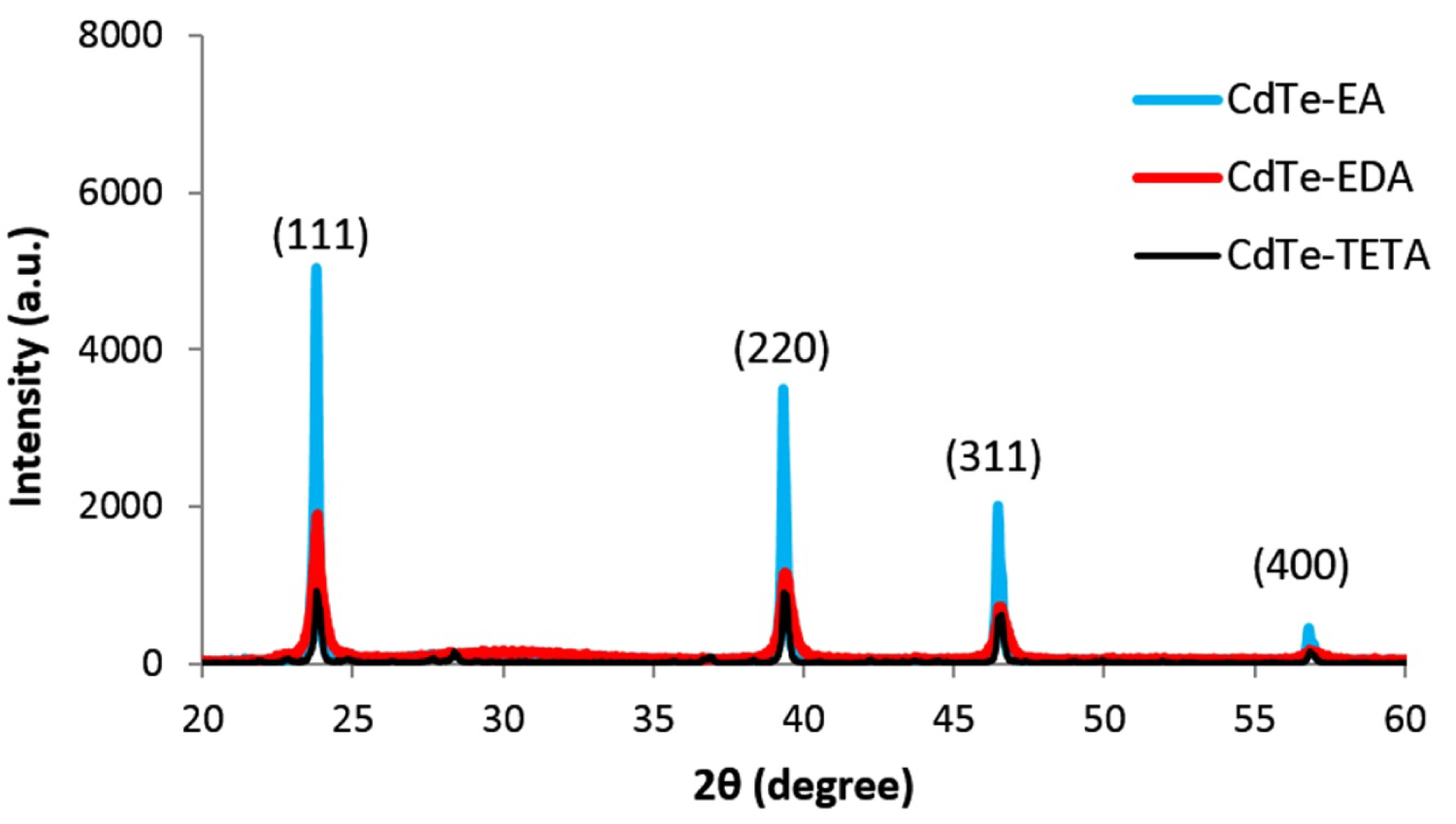
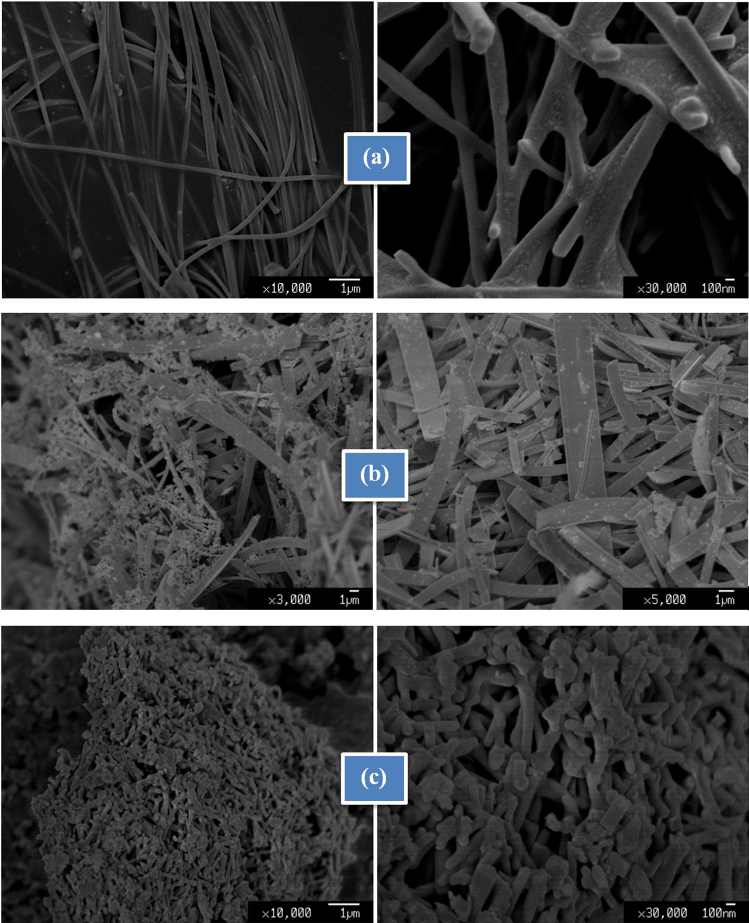
Figure 2: FE-SEM images of CdTe nanostructures synthesized...
FE-SEM images of CdTe nanostructures synthesized in a) Ethylenediamine; b) Ethanolamine and c) Triethylenetetramine.
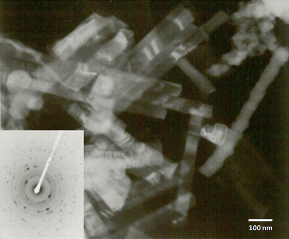
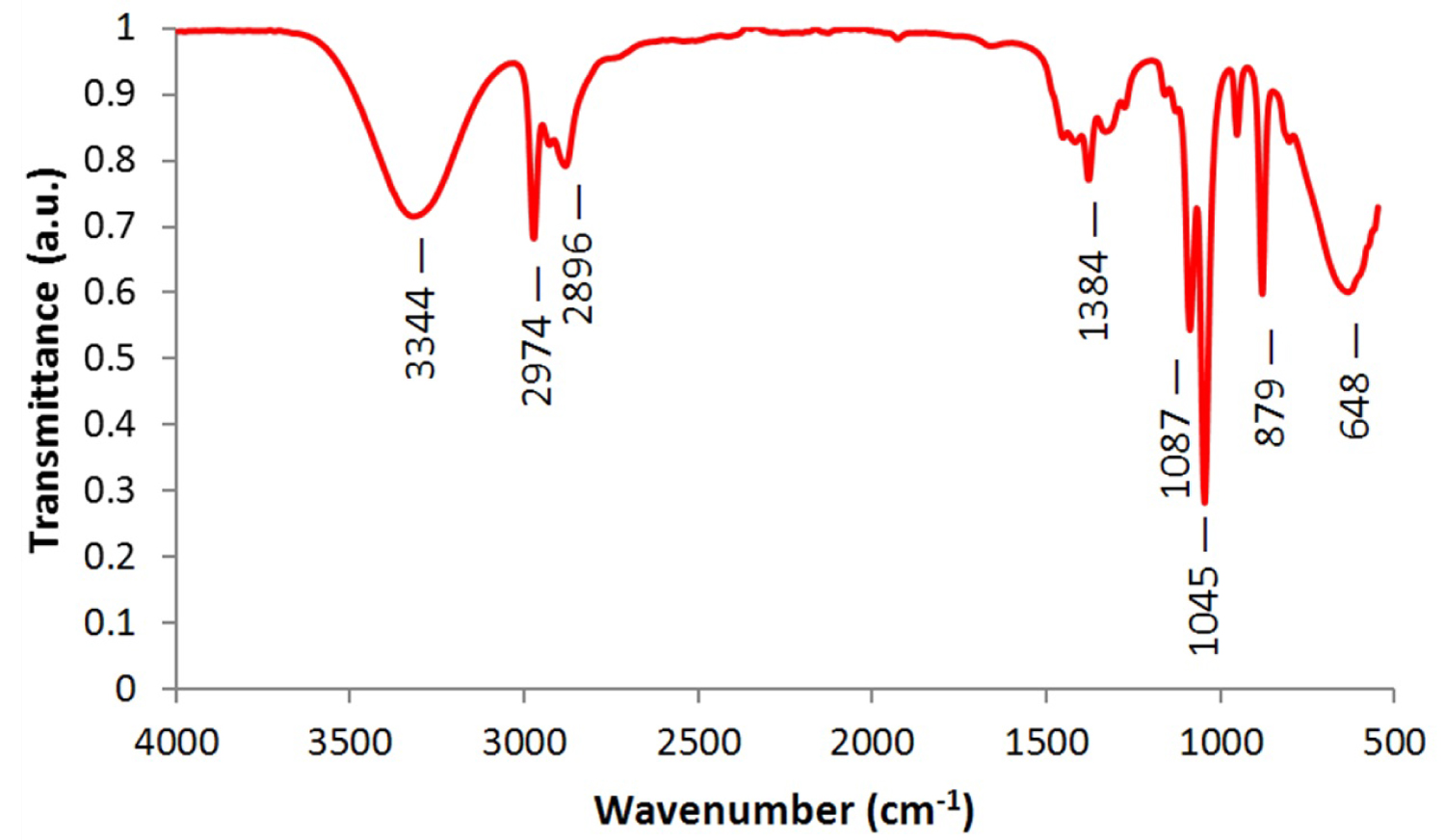
Figure 4: FTIR spectra of the CdTe nanostructures...
FTIR spectra of the CdTe nanostructures solvothermally synthesized.
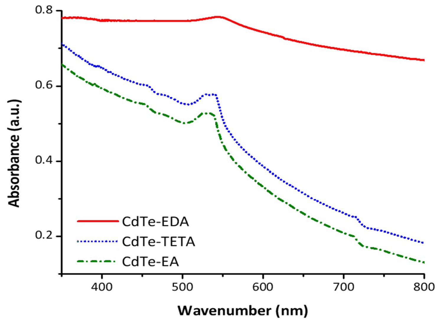
Figure 5: UV-Visible absorption...
UV-Visible absorption spectra of the CdTe nanostructures synthesized in a) Ethylenediamine; b) Ethanolamine and c) Triethylenetetramine.
Tables
Table 1: CdTe nanostructures prepared with various solvents.
Table 2: The structural parameters CdTe with different morphologies.
References
- Campos CEM, Ersching K, Lima JC, Grandi TA, Hohn H, et al. (2008) Influence of minor oxidation of the precursor powders to form nanocrystalline CdTe by mechanical alloying. J Alloys Compd 466: 80-86.
- Zhang X, Xie Y, Zhao Q, Tian Y (2003) 1-D coordination polymer template approach to CdS and HgS aligned-nanowire bundles. New J Chem 27: 827-830.
- Colvin VL, Schlamp MC, Alivisatos AP (1994) Light-emitting diodes made from cadmium selenide nanocrystals and a semiconducting polymer. Nature 370: 354-357.
- Yao J, Zhao G, Han G (2003) Synthesis and characterization of the thiourea-capped CdS nanoparticles. J Mater Sci Lett 22: 1491-1494.
- Soga T (2006) Nanostructured materials for solar energy conversion, Elsevier.
- Heo K, Lee H, Jian J, Lee DJ, Park Y, et al. (2015) Bi-assisted CdTe/CdS hierarchical nanostructure growth for photoconductive applications. Nano Res Lett 10: 331.
- Shao Z, Jie J, Sun Z, Xia F, Wang Y, et al. (2015) MoO3 nanodots decorated CdS nanoribbons for high-performance, homojunction photovoltaic devices on flexible substrates. Nano Lett 15: 3590-3596.
- Wu PC, Ma RM, Liu C, Sun T, Ye Y, et al. (2009) High-performance CdS nanobelt field-effect transistors with high-κ HfO2 top-gate dielectrics. J Mater Chem 19: 2125-2130.
- Ramírez HY, Flórez J, Camacho ÁS (2015) Efficient control of coulomb enhanced second harmonic generation from excitonic transitions in quantum dot ensembles. Phys Chem Chem Phys 17: 23938-23946.
- Carvalho MS, Mayrinck C, Raphael E, Bettini J, Ferraria JL, et al. (2017) The role that electrolytes play in the synthesis of water-soluble CdTe quantum dots prepared at ambient temperature. J Braz Chem Societ 28: 1167-1176.
- Duan XF, Lieber CM (2000) Laser-Assisted Catalytic Growth of single crystal GaN nanowires. J Am Chem Soc 122: 188-189.
- Hu J, Odom TW, Lieber CM (1999) Chemistry and physics in one dimension: Synthesis and properties of nanowires and nanotubes. Acc Chem Res 32: 435-445.
- Yu SH, Wu YS, Yang J, Han ZH, Xie Y, et al. (1998) A novel solvothermal synthetic route to nanocrystalline CdE (E = S, Se, Te) and the Morphological Control. Chem Mater 10: 2309-2312.
- Routkevitch D, Bigioni T, Moskovites M, Xu JM (1996) Electrochemical Fabrication of CdS nanowire arrays in porous Anodic Aluminum Oxide Templates. J Phys Chem 100: 14037-14047.
- Peng XS, Zhang J, Wang XF, Wang YW, Zhao LX, et al. (2001) Synthesis of highly ordered CdSe nanowire arrays embedded in anodic alumina membrane by electrodeposition in ammonia alkaline solution. Chem Phys Lett 343: 470-474.
- Manna L, Scher EC, Alivisatos AP (2000) Synthesis of soluble and processable rod-, arrow-, teardrop-, and tetrapod-shaped CdSe nanocrystals. J Am Chem Soc 122: 12700-12706.
- Chander S, Dhaka MS (2016) Thermal evolution of physical properties of vacuum evaporated polycrystalline CdTe thin films for solar cells. J Mater Sci: Mater Electron 27: 11961-11973.
- Chander S, Purohit A, Lal C, Dhaka MS (2017) Enhancement of optical and structural properties of vacuum evaporated CdTe thin films. Materials Chemistry and Physics 185: 202-209.
- Patel SL, Chander S, Purohit A, Kannan MD, Dhaka MS (2018) Influence of NH4Cl treatment on physical properties of CdTe thin films for absorber layer applications. J Phys Chem Solids 123: 216-222.
- Demazeau G (2008) Solvothermal processes new trends in materials chemistry. J Phys 121: 1-5.
- Wang Q, Pan D, Jiang S, Ji X, An L, et al. (2006) A solvothermal route to size- and shape-controlled CdSe and CdTe nanocrystals. J Cryst Growth 286: 83-90.
- Suriwong T, Phuruangrat A, Thongtem S, Thongtem T (2015) Synthesis, characterization and photoluminescence propertis of CdTe nanocrystals. J Ovonic Res 11: 257-261.
- Scherrer P (1918) Bestimmung der grösse und der inneren struktur von kolloidteilchen mittels röntgenstrahlen. Göttinger Nachrichten Math Phys 2: 98-100.
- Gubur HM, Septekin F, Alpdogan S (2015) CdSe nanowires grown by using chemical bath deposition. J Korean Phys Soc 67: 1222-1227.
- Patel SV, Patel MP, Patel RG (2005) Synthesis and characterization of novel substituted spiro[isobenzofuran-1(3H),9'-xanthene]-3-ones. J Serb Chem Soc 70: 931-936.
- Bai HJ, Zhang ZM, Guo Y, Yang GE (2009) Biosynthesis of cadmium sulfide nanoparticles by photosynthetic bacteria rhodopseudomonas palustris. Colloids Sur B 70: 142-146.
- Bera P, Kim CH, Seok S (2010) High-yield synthesis of quantum-confined CdS nanorods using a new dimeric cadmium (II) complex of S-benzyldithiocarbazate as single-source molecular precursor. Solid State Sci 12: 532-535.
- Chen Z, Dinh HN, Miller E (2013) UV-V is Spectroscopy. In: Photoelectrochemical Water Splitting: Standards, Experimental Methods, and Protocols. Springer, Briefs in Energy, New York, NY, 49-62.
- Olesiak JK, Kloper V, Osovsky R, Sashchiuk A, Lifshitz E (2007) Synthesis and characterization of brightly photoluminescent CdTe nanocrystals. Surf Sci 601: 2667-2670.
- Yao J, Zhao G, Wang D, Han G (2005) Solvothermal synthesis and characterization of CdS nanowires/PVA composite films. J Mater Lett 59: 3652-3655.
Author Details
Shahin Ranjbarzadeh1*, Hamed Omid2 and Naiyer Razmara1,3
1Department of Mechanical Engineering, Escola Politécnica, University of São Paulo, São Paulo, SP, Brazil
2Department of Life Science Engineering, Faculty of New Sciences and Technologies, University of Tehran, Tehran, Iran
3Department of Mechanical Engineering, Azarbaijan Shahid Madani University, Tabriz, Iran
Corresponding author
Shahin Ranjbarzadeh, Department of Mechanical Engineering, Escola Politécnica, University of São Paulo, São Paulo, SP, Brazil.
Accepted: March 04, 2019 | Published Online: March 06, 2019
Citation: Ranjbarzadeh S, Omid H, Razmara N (2019) Facile One-Pot Solvothermal Synthesis of Nanocrystalline CdTe with Different Shapes. Int J Nanoparticles Nanotech 5:023.
Copyright: © 2019 Ranjbarzadeh S, et al. This is an open-access article distributed under the terms of the Creative Commons Attribution License, which permits unrestricted use, distribution, and reproduction in any medium, provided the original author and source are credited.
Abstract
One dimensional Cadmium Telluride (CdTe) with different morphology was successfully synthesized via a solvothermal process by controlling the nature of precursors and solvents at a moderate temperature of 180 ℃. X-ray diffraction (XRD) and Fourier transform infrared (FTIR) spectroscopy analyses revealed that in all cases highly pure and crystallized CdTe with cubic zinc blende structure were obtained. Field emission scanning electron microscope (FE-SEM) analysis revealed that high aspect ratio CdTe nanowires, CdTe nanobelts, and CdTe nanorods were obtained in the presence of ethylenediamine, ethanolamine, and triethylenetetramine, respectively. Also, it was found that the solvents influence on the morphology of CdTe nanostructures. UV-Vis absorption spectra of CdTe nanostructures prepared under different conditions exhibited a blue shift relative to that of bulk CdTe due to the quantum size effect.
Keywords
Cadmium telluride, Synthesis, Solvothermal, Nanobelt, Nanorod, Nanowire
Introduction
The semiconductor nanocrystals have received wide interest for decades due to their exclusive chemical and physical properties, for instance, broadband excitation, narrow bandwidth emission, high photobleaching threshold, superior chemical stability, and tunable spectral properties [1]. The optical, electronic and catalytic characteristics of semiconductor nanocrystals are shape and size-dependent [2]. Cadmium telluride (CdTe) is one of the significant members of the II-VI semiconductor group with an appropriate band gap of 1.475 eV to match the maximum range of the solar spectrum and also has large Bohr radius (7.3 nm) [3,4]. Nanocrystalline CdTe films have potential applications as n-type window layers in solar cells. Moreover, the estimated value of the band gap for these nanostructures has been indicated to be of about 2.8 eV as compared to a bulk CdTe band gap of 1.5 eV [5]. One-dimensional (1D) nanostructures like nanowires, nanorods, and nanobelts have become the focus of research due to their special applications in optoelectronic devices [6,7], solar cells [8], and biological labeling [9].
However, other CdTe nanostructures like CdTe quantum dots synthesized to investigate their optical properties with dispersion in an aqueous medium at ambient temperature [10]. To the present, one dimensional CdTe have been synthesized by different techniques which include laser-assisted catalysis growth (LCG) [11], vapor-liquid-solid (VLS) growth [12], solvothermal route [13], template-assisted technique, electrochemical fabrication [14,15], organometallic [16] and so on. Recent research on the improvement of optical and structural properties of CdTe thin films have been published by Chander, et al. [17,18]. It was found that the estimated crystallographic and optical parameters alter with annealing temperature so that the electrical conductivity increases, and the resistivity decrease with increasing temperature [18]. In another study, these group of researchers explored the physical properties of electron beam processed polycrystalline CdTe thin films considering the influence of NH4Cl activation treatment and thermal evolution. The results exhibited that the NH4Cl treated CdTe thin layers annealed at 320 ℃ is a suitable choice to a p-type absorber layer because of their superior crystallinity, absorbance, and roughness as the prerequisite to designing efficient Cd-based solar cells [19].
The solvothermal technique has been well adapted for a wide range of inorganic crystalline materials. The profound investigations on solvothermal technique have made it an appropriate route for metal chalcogenides synthesis with an ability to control structures and reach to desired properties. This method as a soft chemical route at low temperatures gives aptitude to form a variety of structures without causing any unwanted changes in polychalcogen building-blocks [20]. A solvothermal route was employed to synthesize CdSe and CdTe nanocrystals with toluene as a solvent by studying the size and shape effects [21]. The results indicated that the shape of the resulting zinc blende nanocrystals was controlled mainly by initial precursor concentrations. Recently, CdTe nanocrystals were successfully synthesized from Cd(NO3)2⋅4H2O and Te powder in ethylenediamine (C2H4(NH2)2 by solvothermal reaction at 200 ℃. The product was enumerated as cubic CdTe nanocrystals (41.39 nm) with an emission peak at 550 nm excited by 300 nm wavelength [22]. By the review in the literature, it is obvious that there is a lack of data on the effects of both solvent and shape on the morphology of CdTe nanostructures. In this work, we have synthesized 1D nanostructures with various shapes via employing different solvents. In this one-pot solvothermal method, any reduction or complexing agent is not utilized, and the only parameter is the solvent of the process.
Materials and Methods
Materials
Cadmium chloride (CdCl2, Fluka, 99%) and potassium telluride (KTe, Alfa Aesar, 97%) were used as precursors. Ethylenediamine (Merck, 99%), ethanolamine (Merck, 99%), and triethylenetetramine (Merck, 95%) were employed as solvents. All chemical reagents were of analytical grade and used as were received without additional purification.
Preparation of One dimensional CdTe
In a typical experiment, a mixture of 3 mol CdCl2 and KTe (with a molar ratio of 3:1) was added to 10 mL of the organic solvent and stirred for dissolving salts, and the resultant solution was placed into a 23 mL Teflon-lined stainless-steel autoclave. After autoclave sealing, it was heated up to 180 ℃ for 60 h and then was cooled down to room temperature. The product was accumulated and washed repeatedly with distilled water and absolute ethanol, and next dried in vacuum at 80 ℃. The obtained black powders were collected for characterization. To study the effect of solvent on sample morphology, this experiment was carried out for three different solvents, as presented in Table 1.
Characterization
X-ray diffraction (XRD) patterns of the washed nanopowders were recorded on a Philips X'pert PW3020 X-ray diffractometer with Cu-Kα radiation (1.5418 Å). The crystallite size of CdTe nanocrystals was calculated from their reflections using the Scherrer equation. FTIR bond configurations have examined using Tensor 27 FT-IR spectrometer (Bruker, Germany) in a region of 4000-350 cm-1. Field emission scanning electron microscope (FE-SEM, JEOL JSM-6340F) was employed for the morphological study of the CdTe nanocrystals in different conditions. Transmission electron microscope (TEM, JEOL 200CX) with accelerating voltage of 200 kV was used for size measurement and structure examining. UV-visible absorption spectra were taken by Perkin Elmer Lambda 700 double beam spectrometer.
Results and Discussion
XRD analysis
The XRD patterns of as-synthesized CdTe materials by the solvothermal method using different solvents are shown in Figure 1. It can be noticed that, in all cases, highly pure and crystalline CdTe compounds were formed. All reflections can be indexed to zinc blend structure with F43m space group. The CdTe nanowires solvothermally synthesized in EDA is represented with red color. The calculated zinc blend lattice parameter is 6.476 Å, which is in good agreement with the reported magnitude in JCPDS card no. 15-770 (a = 6.481 Å). The blue and black patterns are related to CdTe nanobelts and nanorods prepared in the presence of EA and TETA with a lattice parameter of 6.470, 6.480 Å respectively. Their measured lattice parameters are also in good consistent with JCPDS. The crystallite size was calculated from FWHM (full-width at half-maximum) values for the (111) peak of the XRD patterns using the Scherrer equation as follows [23]:
Where is the crystalline average size in the direction perpendicular to the lattice planes, hkl are the Miller indices of the analyzed planes; K is the numerical shape factor (Scherrer constant); λ is the wavelength of X-rays; β is the FWHM of the X-ray diffraction peak in radians; and θ is the Bragg angle.
The nanowire, nanobelt, and nanorod samples had crystallite sizes of 69, 83 and 83 nm respectively. Additionally, in all cases, the preferable orientation growth of CdTe on (111) plane (2θ = 23.8°), was observed.
Structural parameters including lattice constant, crystallite size, thickness or diameter, length, dislocation density, number of crystallites per unit area, and internal strain were calculated [18,24] and summarized in Table 2.
FE-SEM and TEM analysis
Figure 2a contains nanowires with a diameter of about 80-150 nm and a length of 30-50 µm. Figure 2b shows the nanobelts with a thickness of 70 nm and a length of 10 µm. Finally, high aspect ratio (< 10) nanorods with an average diameter of 150 nm are shown in Figure 2c.
It is observed from the FE-SEM images that the one-dimensional CdTe synthesized in this work are in three different shapes with various aspect ratios. These results prove the influence of the solvents on the morphology of produced nanostructures.
Figure 3 represents the TEM image of CdTe nanowires obtained by EDA. The TEM images of nanobelts and nanorods were observed to be the same as those of nanowires. CdTe nanowires, with the width and length of 80-110 nm and 400-7000 nm respectively, can be evidently observed. The Selected Area Electron Diffraction Pattern (SAED) for the nanowires shown as the inset in Figure 3, demonstrates that the CdTe nanostructures are polycrystalline with a cubic structure and d-spacing of 3.75 Å, which coincides with the XRD patterns (JCPDS card no. 15-770, d = 3.742 Å).
FTIR analysis
The bond configuration of synthesized CdTe nanostructures is shown in Figure 4. As can be seen for CdTe-EDA nanowires (Figure 4) the following bands obtained: The band appeared at 879 cm-1 can be allocated to stretching vibration of N-H and C=N bonds, respectively [25]. The C-H stretching vibration groups were seen at various wavenumbers, being around 1384 cm-1 corresponding to CH, at 1087 cm-1 and 1045 cm-1 corresponding to CH2 [26]. Additionally, the set of two bands around 2974 cm-1 and 2896 cm-1 is attributed to the O-CH3 stretching vibrations [27]. The broadband located at 3344 cm-1 can be related to the stretching vibration of hydroxyl (O-H) bond. It should be noted that a similar spectrum was obtained for CdTe-EA nanobelts and CdTe-TETA nanorods.
UV-Visible analysis KTe
UV absorption spectra (Figure 5) showed that the products had an optical band edge of approximately 538, 526 and 519 nm which is blue shifted from the 790 nm expected for the bulk material. The computed band gap energies for nanowires, nanobelts, and nanorods were 2.30, 2.36, 2.39 eV, respectively. The band gap energies were calculated from the UV absorption spectra [28]. By the comparison with the previous literature, this enhanced bandgap shows that CdTe nanostructures can be utilized as n-type window layers in p-n homojunction thin-film CdTe solar cells and in electroluminescent display devices. From absorption results, it is obvious that there is a reasonable correlation between the change in aspect ratio of CdTe nanostructures and a shift in the optical band gap. In all cases, the sharpness of the absorption peak points out a narrow size distribution of the synthesized nanostructures [29].
Growth Mechanism
In the present route, the CdTe nanostructures were synthesized from the disproportionation of tellurite as follows:
It can be suggested that EDA plays a crucial role in 1D growth of CdTe crystallites. Tellurium salt decomposes in basic media to release Te2- at high temperature, which bonds with the complexion [Cd(EDA)2]2+ in the solution and then the CdTe nanowires form after losing the volatile EDA molecules at specific temperatures. In the early stage of the CdTe nanowires growth process, only small CdTe crystallites form. With the extended time interval, the small crystallites develop into long nanowires with great aspect ratios. The chemical solution transport growth mechanism can be utilized to describe the results. In the crystal growth, a reversible pathway between the solution phase and the solid phase has a significant role to play. EDA is an intense bidentate solvent which chelates Cd2+ ions thoroughly [30]. This reversible pathway is represented in Eq. (4).
The solvent in the solution phase is inclined to convey the species from the smaller crystallites to the larger ones. In terms of thermodynamic viewpoint, crystal growth can diminish the free energy of the system. The existence of EDA is in favor of the growth of CdTe nanocrystallites in the preferred direction.
" However, TETA with higher molecular weight reduces the aspect ratio of the nanowires. In the presence of TETA concentration of available Te2- ions to combine with Cd2+ increase. This higher concentration encourages isotropic growth which decreases the aspect ratio of nanowires and converts them to the nanorods.
In contrast with EDA and TETA, EA has both amine and hydroxyl group. Moreover, EA has a higher dielectric constant (~37 @ 25 ℃, 1 KHz). This solvent makes an interesting situation which gives two preferred directions to nanocrystals. The first direction is the length of nanobelt and the second is its width. This nanobelt structure can be an exciting option in optical applications.
The FE-SEM micrographs showed various topographies of the products synthesized by the solvothermal method in different solvents. Different CdTe morphologies were formed by altering the solvent due to the distinctive reaction of each solvent with Cd2+.
The unique shape of CdTe nanostructure is related to the strong N-chelating effect of bidentate ligand EDA with Cd2+ and its strong hydrogen binding action effect of the protophilic properties among molecules. EDA has strong coordination ability with Cd2+, which can lead the crystal-growth of CdTe along the [111] orientation.
Conclusions
CdTe nanowires, nanorods and nanobelts have been synthesized by the simple solvothermal method employing cheaper chemicals and various organic solvents, and with better control over the morphology and crystalline quality. Results show that the solvent plays a key role in the solvothermal method and can lead to different morphology of products. The blue shift in the absorption peak of CdTe nanostructures has been confirmed, and the energy gap is found to be 2.37, 2.41 and 2.43 from the absorption spectrum. Besides, the band gaps for nanowires, nanobelts, and nanorods are determined to be 2.30 eV, 2.36 eV, and 2.39 eV, respectively. By the comparison with the previous literature, this improved bandgap reveals that synthesis CdTe nanostructures can be used as n-type window layers in p-n homojunction thin-film CdTe solar cells and in electroluminescent display devices. Present investigation demonstrated that it is possible to synthesis CdTe nanostructures of satisfactory crystalline quality with different morphologies through proper choice of solvents and reagents.