International Journal of Nanoparticles and Nanotechnology
(ISSN: 2631-5084)
Volume 5, Issue 1
Research Article
DOI: 10.35840/2631-5084/5526

Article Formats
Temperature-Dependent Growth of Crystalline Silicon Quantum Dots Embedded in Silicon Nitride
Table of Content
Figures
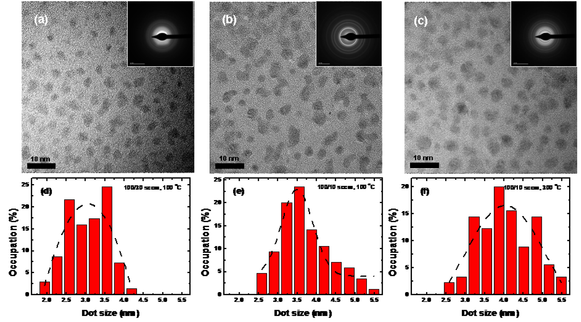
Figure 1: TEM images and TED pattern images...
TEM images and TED pattern images (inset) of samples #1 (a), #2 (b), and #3 (c) and the size distribution of samples #1 (d), #2 (e), and #3 (f), as extracted from this TEM images, for Si QDs. The solid curve is Gaussian curve to fit the size distribution of Si QDs.
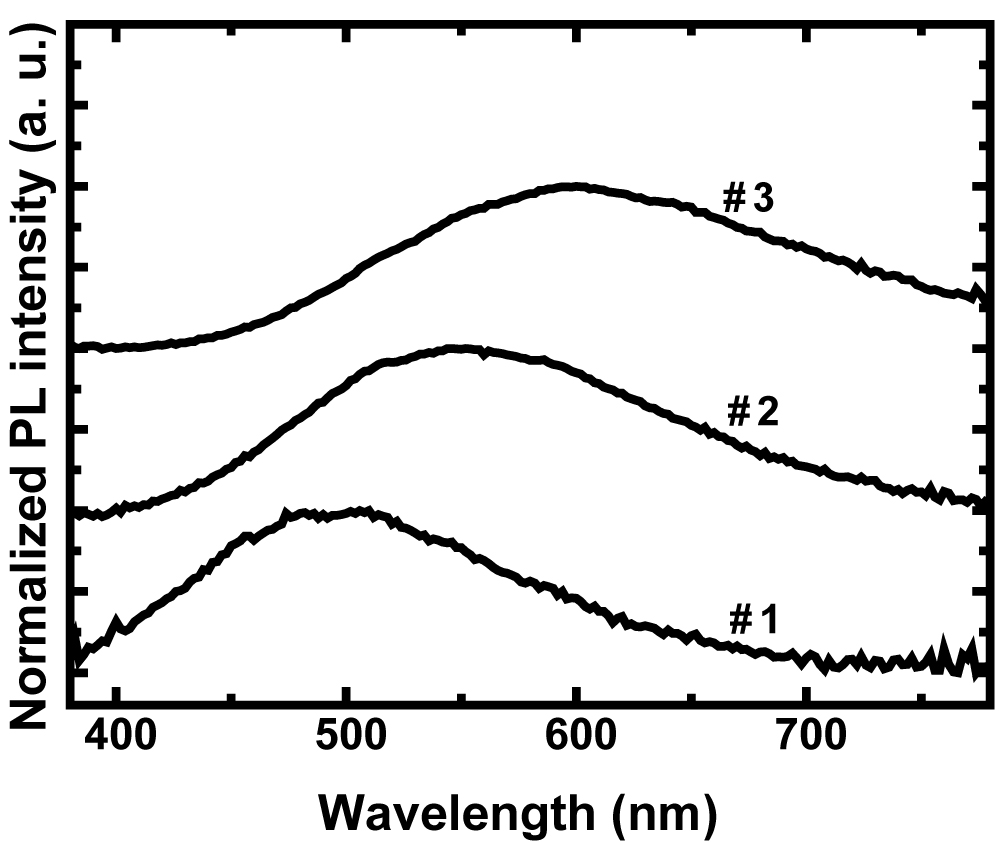
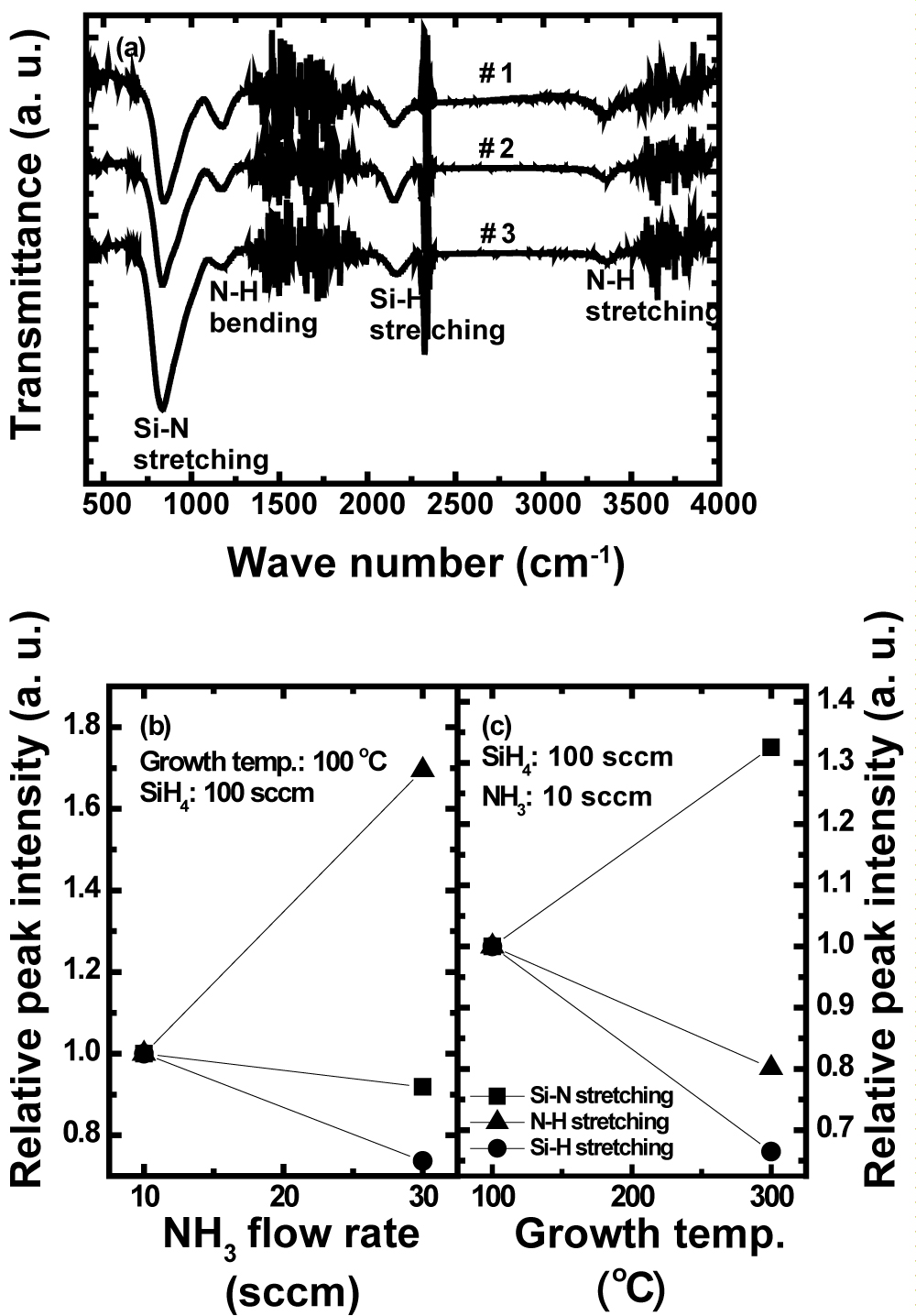
Figure 3: a) FTIR spectra of samples....
a) FTIR spectra of samples #1, #2, and #3; b) Relative FTIR absorption peak intensities as a function of NH3 flow rate. All samples were grown at the temperature of 100 ℃ and SiH4 flow rate of 100 sccm; c) Relative FTIR absorption peak intensities as a function of the growth temperature. All samples were grown at SiH4 flow rate of 100 sccm and NH3 flow rate of 10 sccm.
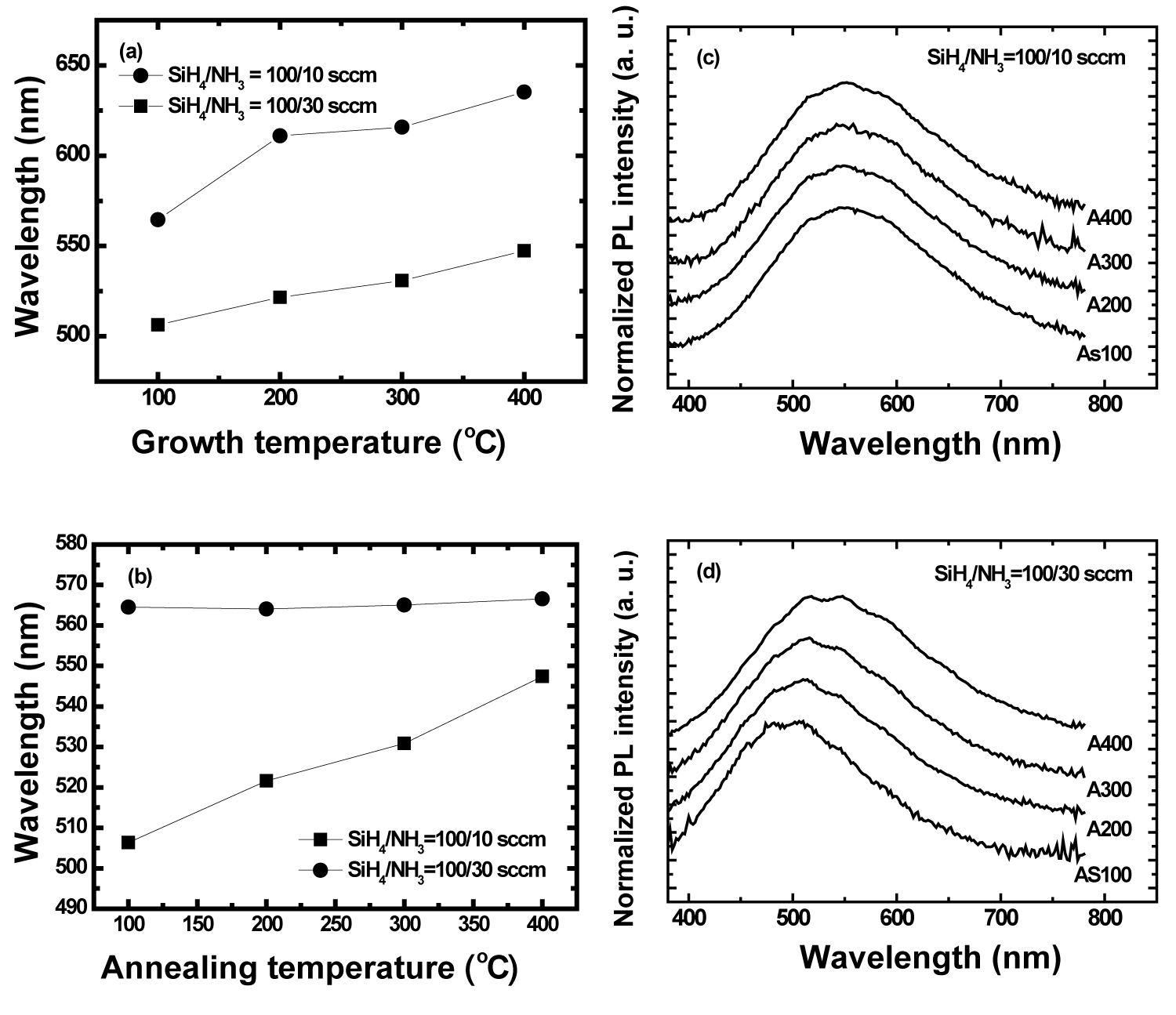
Figure 4: Normalized PL intensities of a) Si QDs....
Normalized PL intensities of a) Si QDs as a function of the growth temperature from 100 to 400 ℃ and b) Annealed Si QDs temperature from 200 to 400 ℃ in PECVD chamber. PL spectra of Si QDs grown using SiH4/NH3 flow rate of 100/10 sccm; c) and 100/30 sccm as a function of annealing temperatures from 200 to 400 ℃ in PECVD chamber. AS100 is the as-deposited sample grown at 100 ℃ (AS100). A200, A300, and A400 are the samples annealed at 200, 300, 400 ℃, respectively.
References
- LT Canham (1990) Silicon quantum wire array fabrication by electrochemical and chemical dissolution of wafers. Appl Phys Lett 57: 1046.
- J Yu, K Chen, Z Ma, X Zhang, X Jiang, et al. (2016) Superior endurance performance of nonvolatile memory devices based on discrete storage in surface-nitrided Si nanocrystals. J Appl Phys 119: 044507.
- NM Park, TS Kim, SJ Park (2001) Band gap engineering of amorphous silicon quantum dots for light-emitting diodes. Appl Phys Lett 78: 2575.
- BH Kim, CH Cho, NM Park, GY Sung, SJ Park (2006) Ni∕Au contact to silicon quantum dot light-emitting diodes for the enhancement of carrier injection and light extraction efficiency. Appl Phys Lett 89: 063509.
- BH Kim, CH Cho, JS Mun, MK Kwon, TY Park, et al. (2008) Enhancement of the external quantum efficiency of a silicon quantum dot light-emitting diode by localized surface plasmons. Adv Mater 20: 3100-3104.
- J Fan, PK Chu (2010) Group IV nanoparticles: synthesis, properties, and biological applications. Small 6: 2080-2098.
- S Furukawa, T Miyasato (1988) Quantum size effects on the optical band gap of microcrystalline Si:H. Phys Rev B: Condens Matter 38: 5726.
- NM Park, CJ Choi, TY Seong, SJ Park (2001) Quantum Confinement in Amorphous Silicon Quantum Dots Embedded in Silicon Nitride. Phys Rev Lett 86: 1355.
- TW Kim, BH Kim, CH Cho, SJ Park (2006) Quantum confinement effect in crystalline silicon quantum dots in silicon nitride grown using SiH4 and NH3. Appl Phys Lett 88: 123102.
- AMP Botas, RAS Ferreira, RN Pereira, RJ Anthony, T Moura, et al. (2014) High Quantum Yield Dual Emission from Gas-Phase Grown Crystalline Si Nanoparticles. J Phys Chem C 118: 10375-10383.
- BH Kim, CH Cho, TW Kim, NM Park, GY Sung, et al. (2005) Photoluminescence of silicon quantum dots in silicon nitride grown by NH3 and SiH4. Appl Phys Lett 86: 091908.
- GN Parsons, JH Souk, J Batey (1991) Low hydrogen content stoichiometric silicon nitride films deposited by plasma‐enhanced chemical vapor deposition. J Appl Phys 70: 1553.
- CH Lin, SC Lee, YF Chen (1993) Strong room‐temperature photoluminescence of hydrogenated amorphous silicon oxide and its correlation to porous silicon. Appl Phys Lett 63: 902.
- A Aydinli, A Serpengüzel, D Vardar (1996) Visible photoluminescence from low temperature deposited hydrogenated amorphous silicon nitride. Solid State Commun 98: 273-277.
- FL Martínez, A del Prado, I Mártil, G González-Diaz, W Bohne, et al. (2001) Molecular models and activation energies for bonding rearrangement in plasma-deposited a-SiNx:H dielectric thin films treated by rapid thermal annealing. Phys Rev B 63: 245320.
- BH Kim, RF Davis, SJ Park (2010) Optical property of silicon quantum dots embedded in silicon nitride by thermal annealing. Thin Solid Films 518: 1744-1746.
- WT Leach, J Zhu, JG Ekerdt (2002) Cracking assisted nucleation in chemical vapor deposition of silicon nanoparticles on silicon dioxide. J Crystal Growth 240: 415-422.
Author Details
Baek Hyun Kim1* and Seong-Ju Park2
1Department of Electrical and Computer Engineering, University of Missouri, Columbia, USA
2Department of Materials Science and Engineering, Nanophotonic Semiconductors Laboratory, Gwangju Institute of Science and Technology, Gwangju, Republic of Korea
Corresponding author
Baek Hyun Kim, Department of Electrical and Computer Engineering, University of Missouri, Columbia, MO 65211, USA.
Accepted: June 03, 2019 | Published Online: June 05, 2019
Citation: Kim BH, Seong-Ju P (2019) Temperature-Dependent Growth of Crystalline Silicon Quantum Dots Embedded in Silicon Nitride. Int J Nanoparticles Nanotech 5:026.
Copyright: © 2019 Kim BH. This is an open-access article distributed under the terms of the Creative Commons Attribution License, which permits unrestricted use, distribution, and reproduction in any medium, provided the original author and source are credited.
The crystalline silicon quantum dots (Si QDs) depending on growth temperature were investigated using plasma enhanced chemical vapor deposition. The size of Si QDs was increased with increasing growth temperature and the ratio between silicon-related gas flow and nitrogen-related gas flow. This is because the growth rate of Si QDs decreases due to surface sites blocking by hydrogen. Hydrogen atoms dissociated from N-H and Si-H could promote the growth of crystalline phase silicon QDs.
Keywords
Silicon nitride, Quantum dot, PECVD, Growth temperature, Crystal
Introduction
Since 1990 [1], silicon quantum dots (Si QDs) have been intensively studied because of the possibility of applications such as compatible metal-oxide-semiconductor (CMOS) devices [2], light source [3-5], fluorescent tags for biomedical applications [6], and their novel applications with electrical and optical functions. For accomplishment of various applications, we need to be trying to understand how to control the size of Si QD embedded in an insulating layer. According to the structural size of Si QD, this is because confined and/or recombined carriers in Si QD represent their different electrical and optical properties [7-10]. However, few papers were reported about the structural properties of Si QDs embedded in silicon nitride. It is necessary that we understand silicon nanostructures to freely control those structures. In this letter, we report on the structural properties of crystalline Si QDs embedded in silicon nitride grown at low temperature.
Experimental
Silicon nitride films containing Si QDs were grown by plasma enhanced chemical vapor deposition (PECVD), in which nitrogen-diluted 5% SiH4 and NH3 were used as the sources of reactants. A low-doped p-type Si wafer (100) with a hole concentration of about 1015 cm-3 was employed as a substrate. Growth temperatures were performed at 100 ℃ and 300 ℃, respectively. For size control of Si QD, NH3 flow rates were changed 10 and 30 sccm fixed SiH4 flow rate of 100 sccm at 300 ℃. The plasma power and chamber pressure were fixed at 10 W and 1 torr. Growth time of all samples was 10 min. A spectral analyzer system was used for the PL measurements at room temperature and a He-Cd 325 nm laser was used as an excitation source. Chemical bonds in the film were examined by a Fourier-transform infrared spectroscopy (FTIR) in the wave number range from 400 to 4000 cm-1 with a resolution of 4 cm-1. The structures of Si QD were investigated by a high-resolution transmission electron microscopy (TEM).
Results and Discussions
To investigate the effect of size distribution of Si QDs, we performed TEM and transmission electron diffraction (TED) analyses of Si QDs embedded in the silicon nitride film in Figure 1a, Figure 1b and Figure 1c and the size distribution of Si QDs was obtained from the TEM image in Figure 1d, Figure 1e and Figure 1f. The growth condition of #1 was the NH3/SiH4 flow rate of 30 sccm/100 sccm and the growth temperature of 100 ℃, while those of #2 and #3 are the NH3/SiH4 flow rate of 30 sccm/100 sccm and the growth temperature of 100 ℃ and 300 ℃, respectively. The average sizes of #1, #2, and #3 were about 3.06, 3.50, and 4.05 nm and the density was similar to about 3 × 10¹² /cm2. Most of Si QD samples were essentially in a crystalline state, as revealed by the electron diffraction patterns showing ring patterns as shown in Figure 1. In previous study [11], we reported that the crystallization of Si QDs is enhanced by the hydrogen dissociated from the NH3 gas. These results reveal that the growth temperature can control the size of Si QDs, while Si QDs are the crystalline phase even at the low temperature.
PL spectra were red-shifted from 506.36 to 564.56 nm with decreasing the flow rate of NH3/SiH4 at 100 ℃ as shown in #1 and #2 of Figure 2. Increasing the growth temperature has also made PL spectra red-shifted from 564.56 to 615.75 nm in the fixed flow rate of gas sources as shown in #2 and #3 of Figure 2. Furthermore, PL spectra of Si QDs are red-shifted with increasing growth temperature with fixed flow rate of NH3/SiH4 (Figure 2b). The shifted PL of Si QDs is in good agreement with TEM analyses grown at various temperatures shown in Figure 1. It is that the shifts of peak positions were reflected as the changed size of Si QD.
The bonding configuration of the film varied with the annealing temperature (Figure 3a). The intense absorption band at 840-870 cm-1 was assigned to the Si-N stretching mode. The band at 3350 cm-1 corresponds to the N-H stretching mode. The band at 2180-2200 cm-1 is the result of the Si-H stretching mode. The relative intensities of the three peaks varied with the changed flow rate of SiH4/NH3 at fixed growth temperature of 100 ℃ and the growth temperature of 100 and 300 ℃. Figure 3b and Figure 3c is a plot of that peak intensities normalized with respect to the as-grown film at 100 ℃ with SH4 flow rate of 100 sccm and NH3 flow rate of 10 sccm, respectively. When the NH3 flow rate was increased, the N-H and Si-H peaks diminished in intensity as the increased temperature promoted the release of hydrogen atoms from N-H and Si-H bonds. When the annealing temperature was increased, the N-H and Si-H peaks diminished in intensity as the increased temperature promoted the release of hydrogen atoms from N-H and Si-H bonds. The Si-N peak intensities decreased slightly with increasing annealing temperature and the peak location was shifted from 841 to 835 cm-1. The reduced Si-N peak intensity suggests that the Si and N atoms released from Si-H and N-H bonds do not rearrange to form Si-N bonds. The changes in the Si-N peak most likely result from decomposition of the silicon nitride matrix [12].
In order to obtain the effect of growth temperature of Si QDs, we performed the annealing of Si QDs grown at 100 ℃ in PECVD chamber. Figure 4a depicts the variation in PL spectra and peak positions for Si QDs embedded in silicon nitride films as the growth temperature was varied between 100 and 400 ℃ in PECVD chamber (Figure 4b). As the growth temperature was increased, the PL peaks were shifted to lower energy values. These clearly show that the shifts of peak positions were reflected as the temperature increase. Figure 4c and Figure 4d shows PL spectra of annealed samples #1 and #2 in the temperature from 100 to 400 ℃ during 10 min. In order to maintain the same growth circumstance, we used PECVD chamber as an annealing furnace. PL peak positions of annealed sample #1 were not changed from 564.56 to 566.6 nm, while those of annealed sample #2 were effectively changed from 506.36 to 547.38 nm. This is because the annealing effect on smaller Si QDs was more effective than that on larger Si QDs due to their surface area-to-volume ratio. In the range of temperature 100 to 400 C, hydrogen atoms between Si QDs and dielectric matrix may be out-diffused and then the formation of new Si-Si atoms between silicon atoms previously bonded to hydrogen by an interchange bond reaction favored by the tendency for chemical order whereby Si-H and Si-N bonds are favored at the expense of N-H and Si-Si bonds [13-16].
The size of Si QD decrease as temperature is lowered. This is because the growth rate of Si QD decreases due to surface site blocking by hydrogen. The growth rate of Si QDs suppressed more significantly than nucleation as temperature drops, thus one obtains the densest and smallest Si QDs at the lowest possible temperature. The selectivity, or relative ability of a precursor to stick to a surface of Si QDs versus a dielectric surface, largely determines density and size of Si QDs. Atomic silicon is nonselective, i.e. it sticks with unit probability to either surface, thus smooth films or very fine polycrystalline films can result [17]. Hydride gases such as silane prefer to adsorb on the Si QD surfaces as opposed to dielectrics, thus sparse nuclei form on the substrate and grow quickly, eventually producing a coarse poly crystalline film.
Conclusion
In this study, the effect on growth temperature of crystalline Si QDs grown using PECVD was investigated. The PL peak positions of Si QDs were red-shifted with increasing the growth temperature. This is attributed to the increase in the size of Si QDs because the Si QDs grown at higher temperature rapidly grew compared to the Si QDs grown at lower temperature due to surface site blocking by hydrogen. The presence of hydrogen atoms during the growth of Si QDs could promote the growth of crystalline phase Si QDs at the even low growth temperature.